65
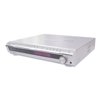
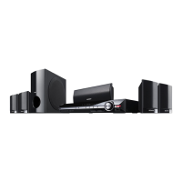
HCD-DX150/DX170/DX250
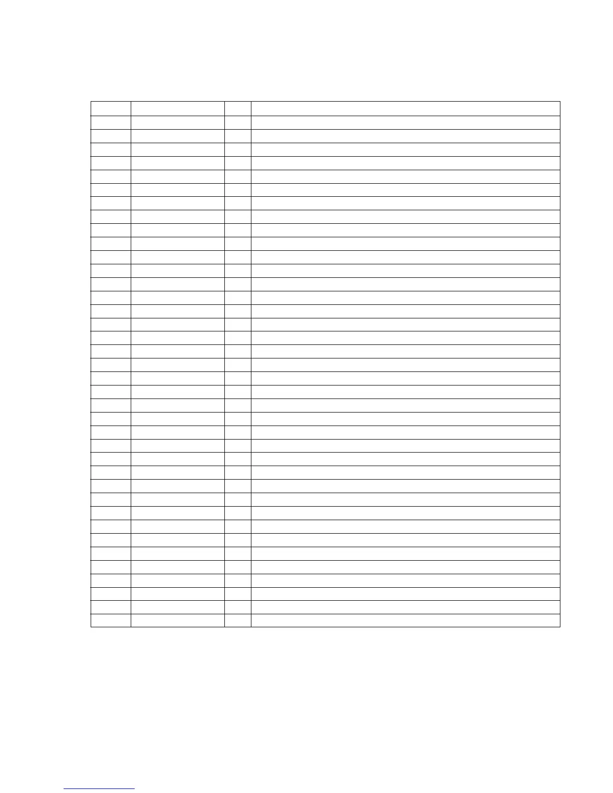
Pin No. Pin Name I/O Description
219 ASDATA2 O Auio serial data
220 XRST — Not Used
221 DVDD18 — Power Supply (+1.8V)
222 ASDATA4 O Auio serial data (not used)
223 DVSS — Terminal Ground
224 DWIDE — Not Used
225 SDPIF — SPDIF output (not used)
226 RFGND18 — Terminal Ground
227 RFVDD18 — Power Supply (+1.8V)
228 ZTALO O Oscillator output signal
229 ZTALI I Oscillator input signal
230 JITFO O RF jitter meter output
231 JITFN I Negative input of operation amplifier for RF jigger meter
232 PLLVSS — Terminal Ground
233 IDAC — Not Used
234 PLLVDD3 — Power Supply (+3.3V)
235 LPFON O Negative output of loop filter amplifier
236 LPFIP I Positive input of loop filter amplifier
237 LPFIN I Negative input of loop filter amplifier
238 LPFOP O Positive output of loop filter amplifier
239 VDD3 I Power Supply (+3.3V)
240 VCM I SACD-Common mode Reference
241 VSS — Terminal Ground
242 VREEP I SACD-TOP Reference
243 VREEN I SACD-Bottom Reference
244 RFVDD3 — Power Supply (+3.3V)
245 RFRPDC I RFRP signal input
246 RFRPAC I RFRP signal input
247 HRFZC I High frequency RF ripple zero crossing
248 CRTPLP O Defect level filter capacitor connecting
249 RFGND — Terminal Ground
250 CEQP O EQ offset loop capacitance (not used)
251 CEQN O EQ offset loop capacitance (not used)
252 OSP O RF offset cancellation capacitor connecting
253 OSN I RF offset cancellation capacitor connecting
254 RFGC O RF offset loop capacitor connecting for DVD-ROM
255 IREF I Current reference input
256 AVDD3 — Power Supply (+3.3V)