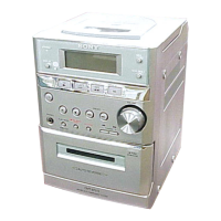
HCD-EH25/EH26
35
USB BOARD IC101 BU9428JKV-E2 (USB CONTROLLER)
Pin No. Pin Name I/O Description
1 RESETX I Reset signal input from the system controller "L": reset
2 SEL_SLAVE I
Mode selection signal input terminal "L": slave mode, "H": stand alone mode
Fixed at "L" in this set
3 SEL_MP3 I
MP3 play mode selection signal input terminal
"L": MP1, MP2 and MP3 play "H": MP3 play only Fixed at "L" in this set
4 SEL_DOUT I
Digital/analog output mode selection signal input terminal
"L": digital output, "H": analog output Fixed at "L" in this set
5 SEL_VOL I
Volume control mode selection signal input terminal
"L": volume control invalid, "H": volume control valid Fixed at "L" in this set
6 SEL_APLAY I
Auto play mode on/off control signal input terminal "L": auto play on, "H": auto play off
Fixed at "H" in this set
7 SEL_UTPKT I
USB test packet output on/off control signal input terminal
"L": USB test packet output on, "H": USB test packet output off Fixed at "H" in this set
8, 9 TEST1, TEST2 - Fixed at "H"
10 MCHNG I Music change signal input from the system controller
11 BUSY O Command operation busy signal output to the system controller
12 SCL I I2C clock signal input from the system controller
13 SDA I/O Two-way I2C data bus with the system controller
14, 15 A0, A1 I I2C slave address signal input terminal Fixed at "L" in this set
16 SEL_SMAN I
Slave mode selection signal input terminal "L": slave mode 3, "H": slave mode 2
Fixed at "H" in this set
17 TEST3 - Not used
18 DVDDIO - Power supply terminal (+3.3V)
19 TEST4 - Not used
20 NC - Not used
21 to 23 TEST6 to TEST8 O Not used
24 DVSS - Ground terminal
25 TEST9 - Not used
26 CLKOUT12 O Clock output terminal (12 MHz) Not used
27 DVDD - Power supply terminal (+1.5V)
28 to 30 TEST11 to TEST13 - Not used
31 ATEST1 - Not used
32 AVDDC - Power supply terminal (+3.3V)
33 USB_DM I/O Two-way data (minus) bus with the USB connector
34 USB_DP I/O Two-way data (plus) bus with the USB connector
35 AVSSC - Ground terminal
36 REXTI I Connect bias resistor to ground terminal
37 VOREFI - Not used
38 VDD_PLL - Power supply terminal (+3.3V)
39 TEST_PLL - Not used
40 XIN_PLL I System clock input terminal (16.9344 MHz)
41 XOUT_PLL O System clock output terminal (16.9344 MHz)
42 VSS_PLL - Ground terminal
43 DAVSS - Ground terminal
44 RDACO O Line output terminal (R-ch) Not used
45 VCDACO O Reference voltage output terminal Not used
46 LDACO O Line output terminal (L-ch) Not used
47 DAVDD - Power supply terminal (+3.3V)
48 AMUTE O Audio muting control signal output terminal Not used
49 to 52 TEST14 to TEST17 - Not used
53 LRCK O I2S clock signal output to the D/A converter
54 BCK O I2S bit clock signal output to the D/A converter
55 DATA O I2S data output to the D/A converter
56 TEST18 - Not used
57 DVDD - Power supply terminal (+1.5V)
58 to 61 TEST19 to TEST22 - Not used
62 DVSS - Ground terminal
 Loading...