EasyManua.ls Logo

Sony HCD-ED2 Service Manual

Sony HCD-ED2
52 pages
To Next Page IconTo Next Page
Page #1 background imageLoading...
Page #1 background image
1
HCD-ED2
US Model
Canadian Model
AEP Model
UK Model
E Model
Australian Model
SPECIFICATIONS
COMPACT DISC DECK RECEIVER
— Continued on next page —
Model Name Using Similar Mechanism NEW
Mechanism Type CDM-61
Base Unit Type KSM-331AAN/K1NP
Optical Pick-up Type KSS-331A (RP)
Model Name Using Similar Mechanism NEW
Tape Transport Mechanism Type CMAL1Z025A
CD
SECTION
TAPE DECK
SECTION
SERVICE MANUAL
HCD-ED2 is the tuner, deck, CD and
amplifier section in CMT-ED2.
Ver 1.2 2004.05
With CORRECTION-1R
(9-929-025-92)
9-929-025-13
2004E02-1
© 2004.05
Sony Corporation
Home Audio Company
Published by Sony Engineering Corporation
This systems is equipped with the Dolby* B-type noise
reduction system.
*Dolby noise reduction manufactured under license
from Dolby Laboratories Licensing Corporation.
“DOLBY” and the double-D symbol a are
trademarks of Dolby Laboratories Licensing
Corporation.
Amplifier section
For the U.S. model
AUDIO POWER SPECIFICATIONS
POWER OUTPUT AND TOTAL HARMONIC
DISTORTION:
With 8-ohm loads both channels driven from
90 - 15,000 Hz; rated 15 watts per channel
minimum RMS power with no more than 09.%
total harmonic distortion from 250 milliwatts to
rated output.
North American model:
Continuous RMS power output (reference):
17 + 17 W
(8 ohms at 1 kHz, 10%THD)
European model:
DIN power output (rated):
15 + 15 W
(8 ohms at 1 kHz, DIN)
Continuous RMS power output (reference):
17 + 17 W
(8 ohms at 1 kHz, 10% THD)
Music power output (reference):
35 + 35 W
Other models:
The following measured at 230 V AC, 60 Hz
DIN power output (rated):
15 + 15 W
(8 ohms at 1 kHz, DIN)
Continuous RMS power output (reference):
17 + 17 W
(8 ohms at 1 kHz, 10%THD)
Inputs
MD IN (phono jacks) :
Sensitivity 1,000 mV, impedance
47 kilohm
CD DIGITAL OUT OPTICAL:
optical
PHONES (stereo phone jack):
Accepts headphones with an
impedance of 8 ohms or more
SPEAKER: Accepts Impedance of 8 to 16
ohms
CD player section
System Compact disc and digital
audio
system
Laser Semiconductor laser
(λ = 780 nm)
Emission duration: continuous
Laser output MAX 44.6 µW*
*This output is the value
measured at a distance of
200 mm from the
objective lens surface on
the Optical Pick-up Block
with 7 mm aperture.
Wavelength 780 - 790 nm
Frequency response
2 Hz - 20 kHz (±0.5 dB)
Tape player section
Recording system 4-track 2-channel stereo
Frequency response (DOLBY NR OFF)
50 - 13,000 Hz (±3 dB),
using a Sony TYPE I cassette
50 - 14,000 Hz (±3 dB),
using a Sony TYPE II cassette
Question and Answer IconNeed help?

Do you have a question about the Sony HCD-ED2 and is the answer not in the manual?

Sony HCD-ED2 Specifications

General IconGeneral
BrandSony
ModelHCD-ED2
CategoryStereo System
LanguageEnglish

Summary

SPECIFICATIONS

CD SECTION SPECIFICATIONS

Technical details for the CD playback section, including output power and impedance.

TAPE DECK SECTION SPECIFICATIONS

Technical details for the tape deck section, including mechanism type.

AMPLIFIER SECTION SPECIFICATIONS

Audio power output and total harmonic distortion specifications for the amplifier.

CD PLAYER SECTION SPECIFICATIONS

Specifications for the CD player, including laser type and frequency response.

TAPE PLAYER SECTION SPECIFICATIONS

Specifications for the tape player, including recording system and frequency response.

SECTION 2 GENERAL

LOCATION OF PARTS AND CONTROLS (FRONT PANEL)

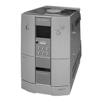
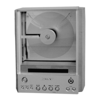
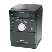
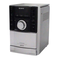
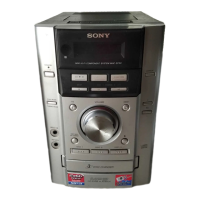
Identification of controls and parts on the front panel of the unit.

LOCATION OF PARTS AND CONTROLS (REMOTE)

Identification of buttons and functions on the remote control.

SAFETY CHECK-OUT

LEAKAGE MEASUREMENT

Procedure for checking AC leakage from exposed metal parts.

OPTICAL PICK-UP BLOCK HANDLING

Notes on safely handling the optical pick-up block to prevent electrostatic breakdown.

LASER DIODE EMISSION CHECK

Guidelines for safely checking the laser diode emission.

SECTION 1 SERVICING NOTE

CD LID OPERATION

Precautions regarding the electrical operation of the CD lid.

SECTION 3 DISASSEMBLY

3-1. CD BASE AND BASE UNIT DISASSEMBLY

Step-by-step instructions for disassembling the CD base and base unit.

3-2. REAR PANEL DISASSEMBLY

Instructions for disassembling the rear panel of the unit.

3-3. BOTTOM COVER AND FRONT PANEL DISASSEMBLY

Procedure for removing the bottom cover and front panel.

3-4. DOOR COVER AND MECHANICAL (CASSETTE) DISASSEMBLY

Steps for disassembling the cassette door cover and mechanical deck.

SECTION 4 MECHANICAL ADJUSTMENTS

MECHANICAL ADJUSTMENT PRECAUTIONS

General precautions before performing mechanical adjustments.

TORQUE MEASUREMENT

Table detailing torque specifications for various mechanical adjustments.

SECTION 5 ELECTRICAL ADJUSTMENTS

DECK SECTION ADJUSTMENT (0 dB=0.775V)

Precautions and settings for deck section electrical adjustments.

RECORD/PLAYBACK HEAD AZIMUTH ADJUSTMENT

Procedure for adjusting the record/playback head azimuth.

TAPE SPEED ADJUSTMENT

Procedure for adjusting the tape speed.

PLAYBACK LEVEL ADJUSTMENT

Procedure for adjusting the playback level for tape.

RECORD BIAS ADJUSTMENT

Procedure for adjusting the record bias.

RECORD LEVEL ADJUSTMENT

Procedure for adjusting the record level.

CD SECTION OPERATION CHECKS

S CURVE CHECK

Procedure for checking the S-curve waveform for focus.

E-F BALANCE (1 TRACK JUMP) CHECK

Procedure for checking E-F balance and waveform levels.

RF LEVEL CHECK

Procedure for checking the RF signal level.

SECTION 6 DIAGRAMS

6-1. CIRCUIT BOARDS LOCATION

Diagram showing the location of various circuit boards.

6-2. SCHEMATIC DIAGRAM – BD SECTION –

Schematic diagram for the BD (Base) board.

6-3. PRINTED WIRING BOARD – BD SECTION –

Printed wiring board layout for the BD section.

6-4. SCHEMATIC DIAGRAM – FUNCTION SECTION –

Schematic diagram for the Function board.

6-5. PRINTED WIRING BOARD – FUNCTION SECTION –

Printed wiring board layout for the Function section.

6-6. SCHEMATIC DIAGRAM – TAPE PREAMP SECTION –

Schematic diagram for the Tape Preamp section.

6-7. PRINTED WIRING BOARD – TAPE PREAMP SECTION –

Printed wiring board layout for the Tape Preamp section.

6-8. SCHEMATIC DIAGRAM – DISPLAY SECTION –

Schematic diagram for the Display section.

6-9. PRINTED WIRING BOARD – DISPLAY SECTION –

Printed wiring board layout for the Display section.

6-10. SCHEMATIC DIAGRAM – RELAY SECTION –

Schematic diagram for the Relay section.

6-11. PRINTED WIRING BOARD – RELAY SECTION –

Printed wiring board layout for the Relay section.

6-12. SCHEMATIC DIAGRAM – POWER SECTION –

Schematic diagram for the Power section.

6-13. PRINTED WIRING BOARD – POWER SECTION –

Printed wiring board layout for the Power section.

6-14. SCHEMATIC DIAGRAM – RDS SECTION –

Schematic diagram for the RDS section.

6-15. PRINTED WIRING BOARD – RDS SECTION –

Printed wiring board layout for the RDS section.

6-16. IC BLOCK DIAGRAMS

Block diagrams illustrating the functionality of key ICs.

6-17. IC PIN FUNCTIONS

Detailed pin assignments and functions for integrated circuits.

SECTION 7 EXPLODED VIEWS

7-1. CD SECTION EXPLODED VIEW

Exploded view of the CD section components.

7-2. REAR PANEL SECTION EXPLODED VIEW

Exploded view of the rear panel components.

7-3. FRONT PANEL SECTION EXPLODED VIEW

Exploded view of the front panel components.

7-4. MECHANISM DECK SECTION (CASSETTE) EXPLODED VIEW

Exploded view of the cassette mechanism deck components.

7-5. BASE UNIT SECTION (CDM-61) EXPLODED VIEW

Exploded view of the CDM-61 base unit components.

SECTION 8 ELECTRICAL PARTS LIST

Related product manuals