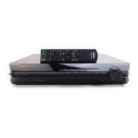
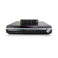
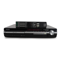
HCD-HDX285/HDX287WC/HDX585/HDX587WC/HDX589W/HDX685/HDX686W
73
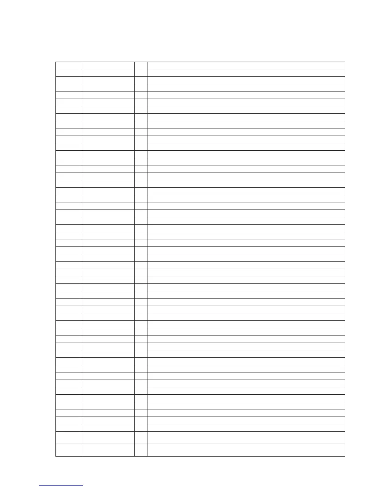
Pin No. Pin Name I/O Description
1 OSN - RF offset cancellation capacitor connecting terminal
2 RFGC O RF AGC loop capacitor connecting terminal for DVD-ROM
3 IREF I Reference current input terminal
4 AVDD3 - Power supply terminal (+3.3V)
5 AGND - Ground terminal
6 DVDA I AC coupled input path A
7 DVDB I AC coupled input path B
8 DVDC I AC coupled input path C
9 DVDD I AC coupled input path D
10 DVDRFP I AC coupled DVD RF signal input from the optical pick-up block
11 MA I DC coupled main-beam RF signal input A
12 MB I DC coupled main-beam RF signal input B
13 MC I DC coupled main-beam RF signal input C
14 MD I DC coupled main-beam RF signal input D
15 SA I DC coupled sub-beam RF signal input A Not used
16 SB I DC coupled sub-beam RF signal input B Not used
17 TNI I 3 beam satellite PD signal negative input from the optical pick-up block
18 TPI I 3 beam satellite PD signal positive input from the optical pick-up block
19, 20 MDI1, MDI2 I Laser power monitor input from the optical pick-up block
21 LDO2 O Laser diode drive signal output to the optical pick-up block (for DVD)
22 LDO1 O Laser diode drive signal output to the optical pick-up block (for CD)
23 SVDD3 - Power supply terminal (+3.3V)
24 CSO O Central servo signal output terminal Not used
25 RFLVL O RFRP low pass output terminal Not used
26 SGND - Ground terminal
27 V2REFO O Reference voltage (+2.8V) output terminal Not used
28 V2O O Reference voltage (+2V) output to the optical pick-up block
29 VREFO O Reference voltage (+1.4V) output terminal
30 FEO O Focus error monitor output terminal Not used
31 TEO O Tracking error monitor output terminal Not used
32 TEZISLV O Tracking error slicing level output terminal Not used
33 OP_OUT O Output from the internal operational amplifi er Not used
34 OP_INN I Negative input to the internal operational amplifi er Not used
35 OP_INP I Positive input to the internal operational amplifi er Not used
36 DMO O Spindle motor control signal output to the motor driver
37 FMO O Sled motor control signal output to the motor driver
38 TROPENPWM O Loading motor control signal output terminal Not used
39 IOPMON I Power monitor terminal
40 TRO O Tracking coil control signal output to the coil driver
41 FOO O Focus coil control signal output to the coil driver
42 AGND18 - Ground terminal
43 AVDD18 - Power supply terminal (+1.8V)
44 USB_DP I/O USB communication data (+) input/output terminal Not used
45 USB_DM I/O USB communication data (-) input/output terminal Not used
46 USB_VDD3 - Power supply terminal (+3.3V)
47 USB_VSS - Ground terminal
48 PAD_VRT I/O USB generating reference current input/output terminal Not used
49 USB_VDD18 - Power supply terminal (+1.8V)
50 USB_VSS - Ground terminal
51 DIR_ERROR I
PLL lock error signal and input data error detection signal input from the digital audio inter-
face receiver "H": error
52 DIR_AUDIO I
PCM/Non PCM detection signal input from the digital audio interface receiver
"L": PCM, "H": Non PCM
MAIN BOARD IC1101 CXD9917R-A (240V AC area in E and Saudi Arabia models),
CXD9927R-A (US and Canadian models)
(RF AMP, SERVO DSP, MPEG DECODER, HDMI TRANSMITTER)
 Loading...