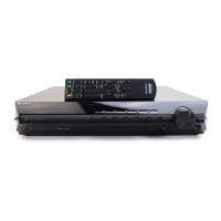
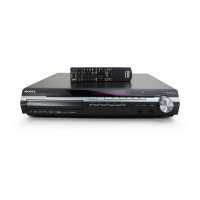
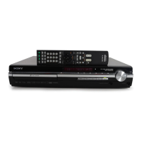
HCD-HDX285/HDX287WC/HDX585/HDX587WC/HDX589W/HDX685/HDX686W
74
Pin No. Pin Name I/O Description
53 LIMITSW I Limit detection switch input terminal
54 MSW O CD/DVD selection signal output terminal "L": CD, "H": DVD
55 DVDD18 - Power supply terminal (+1.8V)
56 to 64
HA2 to HA8,
HA18, HA19
O Address signal output to the fl ash ROM
65 DVDD3 - Power supply terminal (+3.3V)
66 XWR O Write enable signal output to the fl ash ROM
67 to 75 HA16 to HA9, HA20 O Address signal output to the fl ash ROM
76 XROMCS O Chip select signal output to the fl ash ROM
77 HA1 O Address signal output to the fl ash ROM
78 XRD O Read enable signal output to the fl ash ROM
79, 80 HD0, HD1 I/O Two-way data bus with the fl ash ROM
81 DVSS - Ground terminal
82 to 86 HD2 to HD6 I/O Two-way data bus with the fl ash ROM
87 HA21 O Address signal output to the fl ash ROM
88 RESERVED O Not used
89 HD7 I/O Two-way data bus terminal with the fl ash ROM
90 DVSS - Ground terminal
91, 92 HA17, HA0 O Address signal output to the fl ash ROM
93 DVDD18 - Power supply terminal (+1.8V)
94 FWD O Loading motor drive signal output terminal (forward direction) Not used
95 REV O Loading motor drive signal output terminal (reverse direction) Not used
96 DVDD3 - Power supply terminal (+3.3V)
97 IFSDO O Serial data output to the system controller
98 IFCK O Serial data transfer clock signal output to the system controller
99 xIFCS O Chip select signal output to the system controller
100 IFSDI I Serial data input from the system controller
101 SCL O Serial data transfer clock signal output to the EEPROM
102 SDA I/O Two-way data bus with the EEPROM
103 CKSW I Chucking detection switch input terminal Not used
104 OCSW I Disc tray open/close detection switch input terminal Not used
105 RXD I Receive data for fl ash writing input terminal
106 TXD O Transmission data for fl ash writing output terminal
107 ICE I ICE mode enable signal input terminal Not used
108 xSYSRST I Reset signal input from the system controller "L": reset
109 RESERVED I Not used
110 IFBSY I Busy signal input from the system controller
111 DQM0 O Data mask signal output to the SD-RAM
112 EEWP O Write protect signal output to the EEPROM
113 to 117 RD7 to RD3 I/O Two-way data bus with the SD-RAM
118 DVDD3 - Power supply terminal (+3.3V)
119 to 129
RD2 to RD0,
RD15 to RD8
I/O Two-way data bus with the SD-RAM
130 TSD_M O Thermal shut down signal output to the coil/motor driver
131 DVDD3 - Power supply terminal (+3.3V)
132 DQM1 O Data mask signal output to the SD-RAM
133 RWE# O Write enable signal output to the SD-RAM
134 CAS# O Column address strobe signal output to the SD-RAM
135 RAS# O Row address strobe signal output to the SD-RAM
136 RCS# O Chip select signal output to the SD-RAM
137, 138 BA0, BA1 O Bank address signal output to the SD-RAM
139 to 141 RA10, RA0, RA1 O Address signal output to the SD-RAM
142 DVDD18 - Power supply terminal (+1.8V)
143, 144 RA2, RA3 O Address signal output to the SD-RAM
145 DVDD3 - Power supply terminal (+3.3V)
146 DRCLK O Serial data transfer clock signal output to the SD-RAM
 Loading...