47
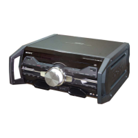
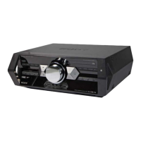
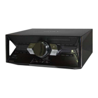
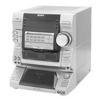
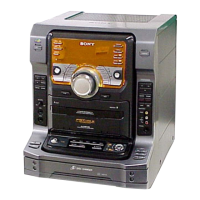
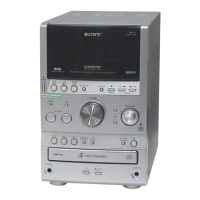
HCD-SPZ90DAB
Pin No.
Pin Name I/O Description
92
SVDD - Power supply terminal (+2.5V)
93
JTAGTCK I Clock signal input terminal (for JTAG) Not used
94
JTAGTDI I Data input terminal (for JTAG) Not used
95
JTAGTDO O Data output terminal (for JTAG) Not used
96
JTAGTMS I Mode select signal input terminal (for JTAG) Not used
97
TRST I Reset signal input terminal (for JTAG) Not used
98
VSS - Ground terminal
99
VDD - Power supply terminal (+1.8V)
100
IOVDD2 - Power supply terminal (+3.3V)
101 DOUT O
Digital audio signal output terminal Not used
102 TEST I
Input terminal for the test Normally: fixed at "L"
103 TES1 I
Input terminal for the test Normally: fixed at "L"
104
IOVSS2 - Ground terminal
105
PLLVDD - Power supply terminal (+1.8V)
106
PLLVSS - Ground terminal
107
XVSS - Ground terminal
108
XTAO O System clock output terminal (16.9344 MHz)
109
XTAI I System clock input terminal (16.9344 MHz)
110
XVDD - Power supply terminal (+1.8V)
111
AVDD1 - Power supply terminal (+3.3V)
112
AOUT1 O L-ch analog audio signal output terminal
113
VREFL O L-ch reference voltage output terminal
114
AVSS1 - Ground terminal
115
AVSS2 - Ground terminal
116
VREFR O R-ch reference voltage output terminal
117
AOUT2 O R-ch analog audio signal output terminal
118
AVDD2 - Power supply terminal (+3.3V)
119
IOVDD0 - Power supply terminal (+3.3V)
120
IOVSS0 - Ground terminal
 Loading...