58
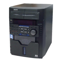
HCD-VM330AV
Pin No. Pin Name I/O Description
46 BUS XWRL O
Not used
47 LO.BOOST O
Low boost control signal output terminal Not used (open)
48
AUDIO MUTING
O
Audio muting on/off control signal output terminal “L”: muting on Not used (open)
49 LOAD OUT O
Loading motor drive signal output terminal Not used (open)
50 LOAD IN O
Loading motor drive signal output terminal Not used (open)
51 INSW I
Disc detection (load in) switch input terminal Not used (fixed at “H”)
52 OUTSW I
Disc detection (load out) switch input terminal Not used (open)
53 MODEL1 I
Destination setting terminal (open)
54 MODEL2 I
Destination setting terminal (open)
55 TBLL O
Table motor drive signal output terminal Not used (open)
56 TBLR O
Table motor drive signal output terminal Not used (open)
57 to 59 ENC1 to ENC3 I
Disc tray address detection signal input terminal Not used (open)
60, 61 — O
Not used (open)
62 VCC —
Power supply terminal (+5V)
63 — O
Not used (open)
64 VSS —
Ground terminal
65 V.MUTE O
Video muting on/off control signal output to the Y/C decoder (IC304) “L”: muting on
66 DAC RESET O
Reset signal output to the D/A converter (IC509)
67 to 72 A5 to A0 O
Address signal output for the external device Not used (open)
73 TEST LED O
LED drive signal output for the self diagnosis indicator Normally: “L” (LED on)
74 TEST1 I
Setting terminal for the test mode 1 (for VCD check)
Normally: fixed at “H” (“L”: test mode)
75 TEST2 I
Setting terminal for the test mode 2 (for SERVO check)
Normally: fixed at “H” (“L”: test mode)
76 TEST3 I
Setting terminal for the test mode 3 Normally: fixed at “H” (“L”: test mode)
Not used (fixed at “H”)
77 DEVICE RESET O
System reset signal output to the CXD3068Q (IC101) and AN41020A (IC102) “L”: reset
78 STANDBY O
Standby on/off control signal output terminal Not used (open)
79 FL CS O
Chip select signal output terminal Not used (open)
80 OFF OUT O
Blank control signal output terminal Not used (open)
81 LPH O
Laser power control signal output terminal Not used (open)
82 LD ON O
Laser on/off selection signal output to the CXA2581N (IC103) “H”: laser on
83 SUBQ CLK O
Subcode Q data reading clock signal output to the CXD3068Q (IC101)
84 SUBQ DATA I
Subcode Q data input from the CXD3068Q (IC101)
85 CL680 HRDY I
Ready status detection signal input from the CL680T (IC505)
86 CL680 RESET O
Reset signal output to the CL680T (IC505) “L”: reset
87 CL680 HSEL O
Command selection signal output to the CL680T (IC505)
88 DF LATCH O
Serial data latch pulse output to the D/A converter (IC509) “L” active
89 MIC CTRL O
Mic control signal output terminal Not used (open)
90 to 92 KEY1 to KEY3 I
Key input terminal Not used (open)
93 NT/PAL I
Video system (NTSC/PAL) select signal input terminal
94 MUSIC VOL I
Volume input terminal Not used (open)
95 DSP DATA O
Serial data output to the CXD3068Q (IC101)
96 AVSS —
Ground terminal (for A/D conversion)
97 DSP LATCH O
Serial data latch pulse output to the CXD3068Q (IC101)
98 VREF I
Reference voltage (+5V) input terminal (for A/D conversion)
99 AVCC —
Power supply terminal (+5V) (for A/D conversion)
100 AMP.ON O
Power amplifier on/off selection signal output terminal Not used (open)
w
w
w
.
x
i
a
o
y
u
1
6
3
.
c
o
m
Q
Q
3
7
6
3
1
5
1
5
0
9
9
2
8
9
4
2
9
8
T
E
L
1
3
9
4
2
2
9
6
5
1
3
9
9
2
8
9
4
2
9
8
0
5
1
5
1
3
6
7
3
Q
Q
TEL 13942296513 QQ 376315150 892498299
TEL 13942296513 QQ 376315150 892498299
http://www.xiaoyu163.com
http://www.xiaoyu163.com