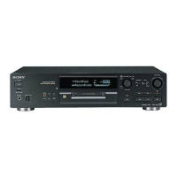
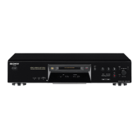
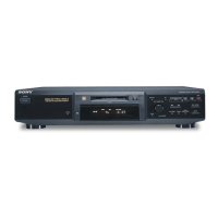
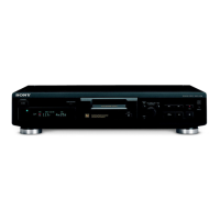
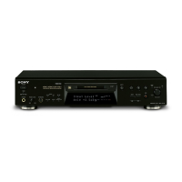
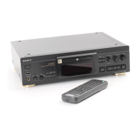
MDS-JB730
– 49 –
– 50 –
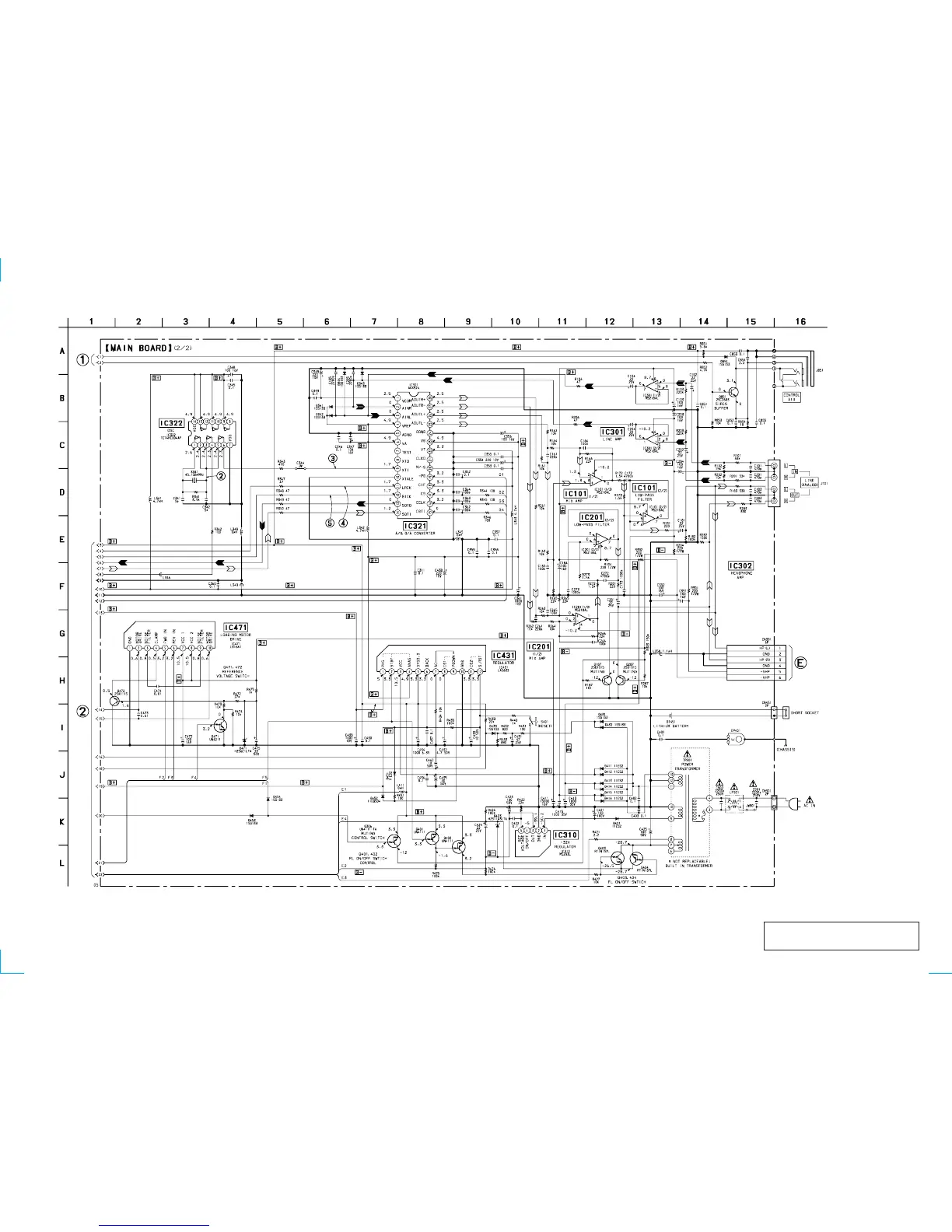
6-11. SCHEMATIC DIAGRAM – MAIN Board (2/2) – • See page 43 for Waveforms. • See page 57 for IC Block Diagrams.
• Voltages and waveforms are dc with respect to ground
under no-signal conditions.
no mark : PLAY
The components identified by mark ! or dotted
line with mark ! are critical for safety.
Replace only with part number specified.
(Page 48)
(Page
48)
(Page 54)
 Loading...