6161
MXD-D4
*
*
*
*
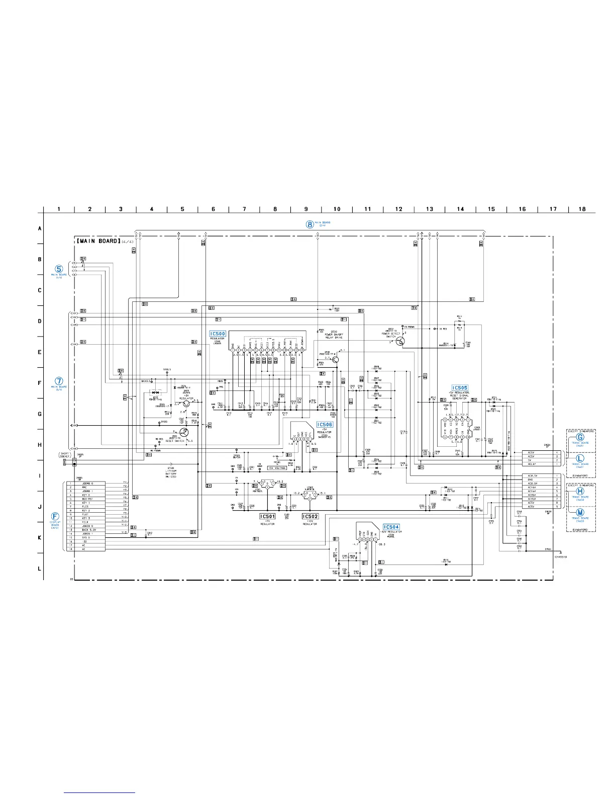
6-15. SCHEMATIC DIAGRAM – MAIN Board (4/4) –• See page 68 for IC Block Diagrams.
Note on Schematic Diagram:
• Voltages and waveforms are dc with respect to ground
under no-signal conditions.
no mark : MD, CD STOP
(Page
63)
(Page 60)
(Page 58)
(Page 59)
(Page 65)
(Page 67)
(Page 65)
(Page 67)
Note: Be sure to execute the Voltage Adjustment on page 44, whenever the asterisked parts (IC506, R550, R551, RV500), mounted
MAIN board, and CD base unit (BU-21BD53) were replaced.
 Loading...