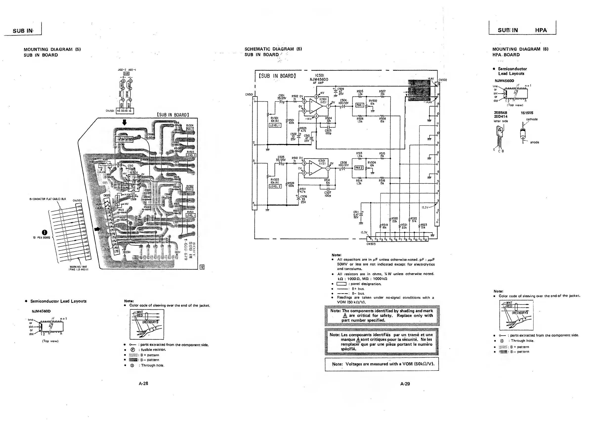
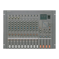
SUB
IN
MOUNTING DIAGRAM (S)
SUB
IN BOARD
SCHEMATIC DIAGRAM
(5)
SUB
IN
BOARD
SUBIN HPA
MOUNTING DIAGRAM
(6)
HPA BOARD
J
102-2
JI02-I
•
Semiconductor
Lead Layouts
NJM4560D
Note:
•
Color
code of
sleeving
over the end
of
the
jacket.
• o
—
:
parts
extracted from
the
component side.
•
©
:
fusible
resistor.
•
:
B +
pattern
•
H13
: B
—
pattern
•
®
: Through
hole.
Note:
•
All
capacitors are in
n
F
unless
otherwise noted.
pF
:
ppF
50WV or less are not
indicated except for electrolytics
and tantalums.
All resistors are
in ohms, %W
unless otherwise
noted.
k«
: lOOOfi,
Mn : lOOOkB
:
panel
designation.
B+ bus.
B- bus.
Readings
are
taken under
no-signal conditions with
a
VOM
(50 kn/V).
Note: The components identified
by shading and
mark
are
critical for safety. Replace only with
part number
specified.
Note: Les
composants identifies par un trame
et
une
marque ^sont critiques
pour
la securite. Ne
les
remplacer
que
par une
piece
portant le numero
specifie.
Note:
Voltages are
measured with a VOM (50k£2/V).
•
Semiconductor
Lead
Layouts
NJM45600
(Top
view)
2SBS48
1S1555
2S0414
Note:
•
Color code of
sleeving over the
end of
the
jacket.
• o—
:
parts
extracted from the
component
side.
•
®
: Through hole,
•
:
B +
pattern
•
B
-
pattern
A-28
A-29