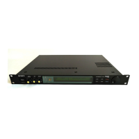
PCM-D50
54
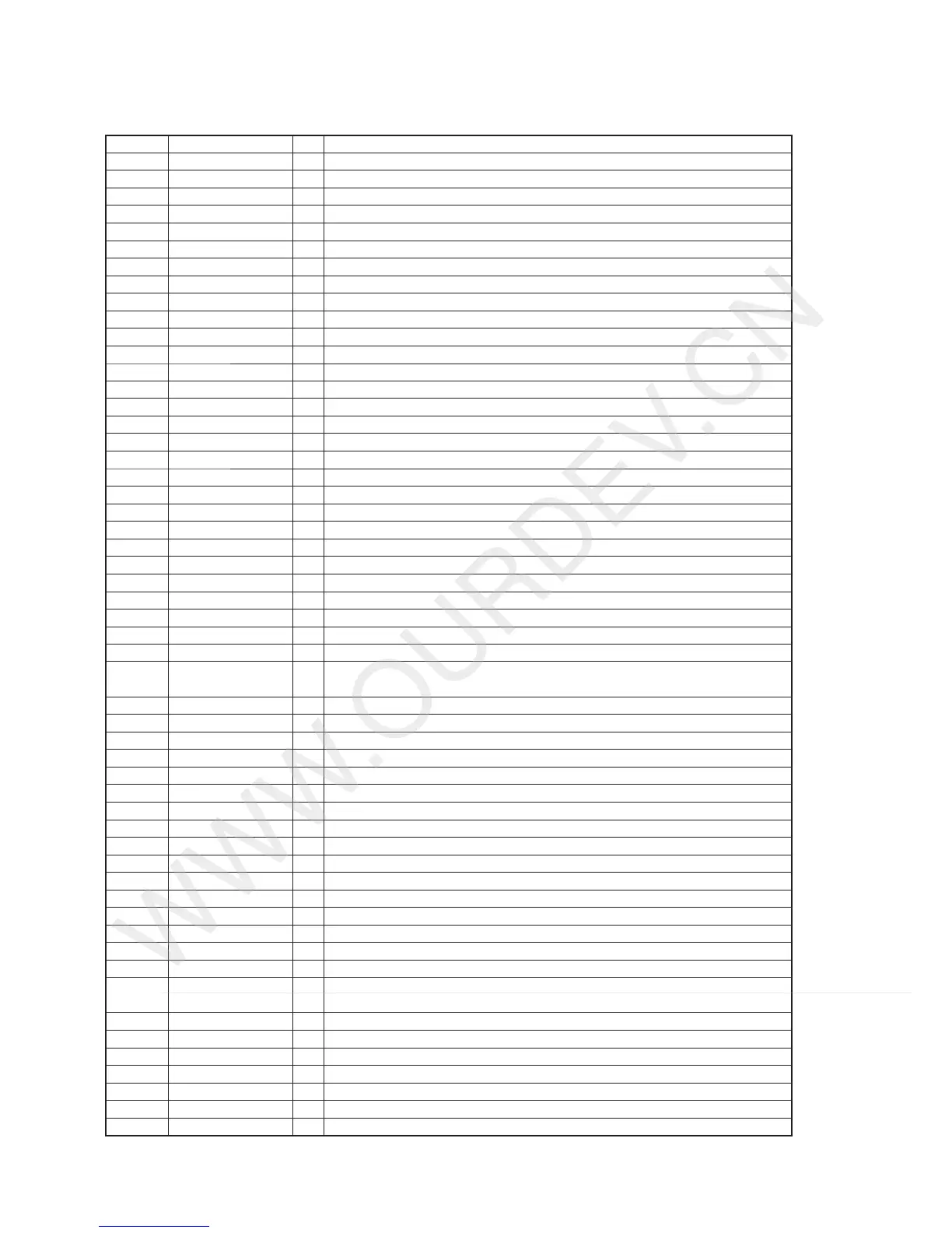
Pin No.Pin NameI/O Description
C15 SWADP — Not used (Open)
C16 CAPVBDL — Not used (Open)
C17VCCVBAT1 — Power supply (battery)
C18 USBTEST3 — Not used (Open)
C19 IO_A — Power supply (VDD_GP1)
C20 AB0_A5OAddress signal output to the USB I/F
C21, C22AB0_A10, AB0_A15 — Not used (Open)
C23, C24AB0_A19, AB0_A23 — Not used (Open)
C25 AB0_D1I/ODate input/output with the USB I/F
C26 NC — Not used (Open)
D1 IDPULLUP — Not used (Pull Down)
D2NAND_RBZ0ORead/busy signal output to the NAND ROM
D3 NAND_ALEOAddress latch enable signal output to the NAND ROM
D4 NAND_DA2I/ODate input/output with the NAND ROM
D5 IO_B — Power supply (VDD_GP1)
D6, D7 VDD_L1 — Power supply (VDD_L1)
D8 GND — Ground
D9 EXTVBUS — Not used (Open)
D10 USB_NXT — Not used (Connected ground)
D11 USB_STB — Not used (Open)
D12USB_DATA1 — Not used (Open)
D13USB_DATA3 — Not used (Open)
D14USB_DATA6 — Not used (Open)
D15 SWVBUS2 — Not used (Open)
D16 CAPVBSW — Not used (Open)
D17VCCVBAT1 — Power supply (battery)
D18 AB0_A3OAddress signal output to the USB I/F
D19 IO_A — Power supply (VDD_GP1)
D20 AB0_A6OAddress signal output to the USB I/F
D21, D22,
D23
AB0_A11, AB0_A16,
AB0_A23
— Not used (Open)
D24, D25AB0_D0, AB0_D2I/ODate input/output with the USB I/F
D26 IMONT — Not used (Open)
E1DISCHGVBUS — Not used (Pull Down)
E2 VBUSV — Not used (Open)
E3 NAND_REZORead enable signal output to the NAND ROM
E4 NAND_DA3I/ODate input/output with the NAND ROM
E5 IO_B — Power supply (VDD_GP1)
E6 NAND_DA5I/ODate input/output with the NAND ROM
E7 NAND_DA8OHeadphone mute signal output
E8 NAND_DA7I/ODate input/output with the NAND ROM
E9 NAND_CLEOCommand latch enable signal output to the NAND ROM
E10 BATSEL IBattery detect signal input
E11 SWBAT — Not used (Open)
E12, E13CAPBTDL, CAPADDL — Not used (Open)
E14USB_DATA7 — Not used (Open)
E15 SWVBUS — Not used (Open)
E16, E17
USBTEST2,
USBTEST1
— Not used (Open)
E18 AB0_A4OAddress signal output to the USB I/F
E19AB0_FLASHCLK — Not used (Open)
E20, E21AB0_A7, AB0_A12 — Not used (Open)
E22 AB0_CSZ1 — Not used (Open)
E23 AB0_A22 — Not used (Open)
E24AB0_A25/DPQIDMA request signal input from the USB I/F
E25 AB0_D4I/ODate input/output with the USB I/F
WWW.OURDEV.CN
 Loading...