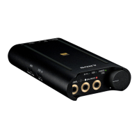
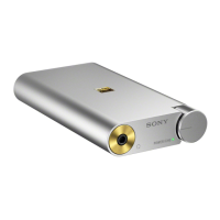
PHA-1A/1AEU
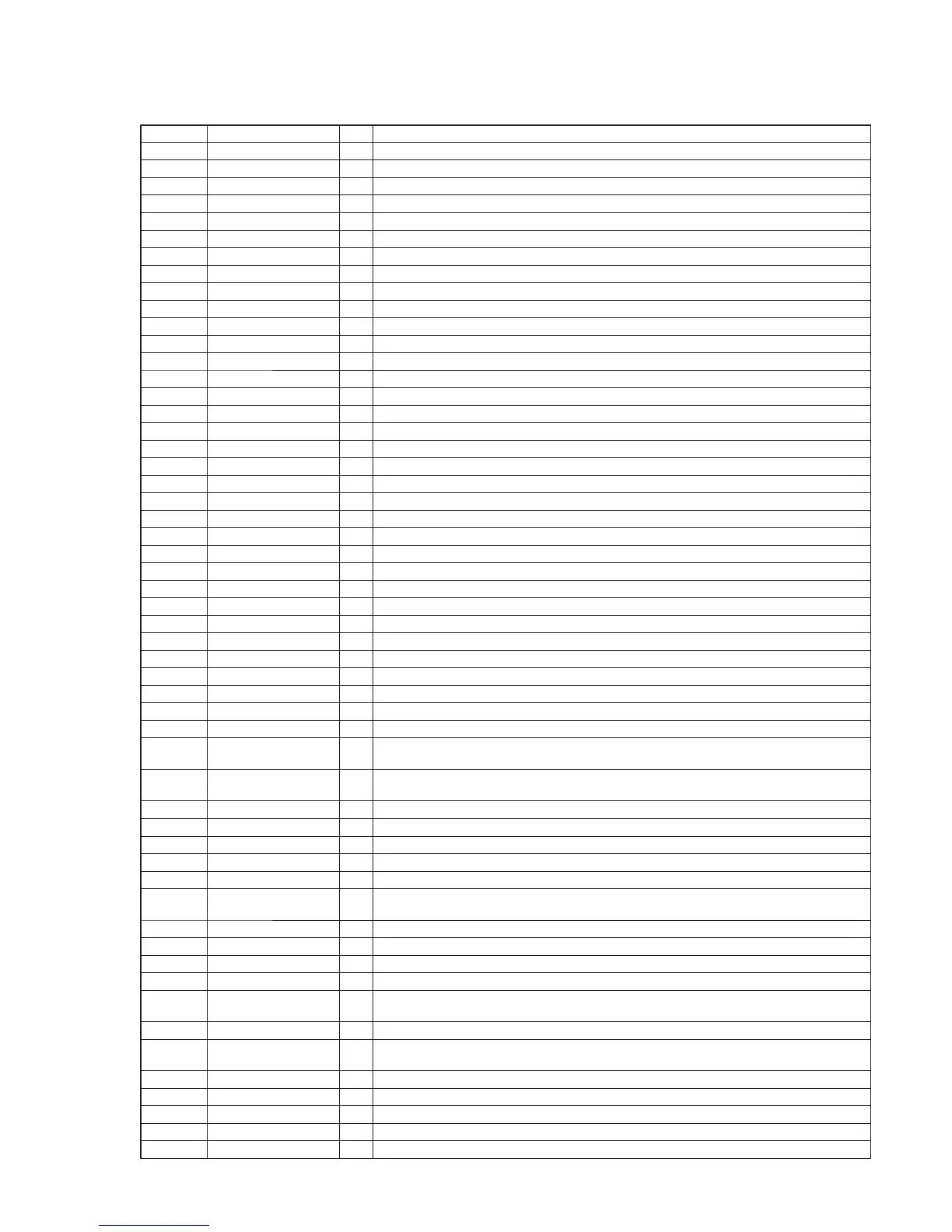
19
Pin No. Pin Name I/O Description
1 XSC0 O System clock output terminal (12 MHz)
2 VCCHSRT - Power supply terminal (+3.3V) (analog system)
3 GNDHSRT - Ground terminal (analog system)
4 RREF I External reference resistor connection terminal
5 USBDM I/O Two-way USB data (–) bus with the INPUT (for PC/WALKMAN/Xperia) connector
6 USBDP I/O Two-way USB data (+) bus with the INPUT (for PC/WALKMAN/Xperia) connector
7 VCCA_U20 - Power supply terminal (+3.3V) (analog system)
8 GNDA_U20 - Ground terminal (analog system)
9 VCC3V - Power supply terminal (+3.3V) (digital system)
10 VCC O External fi lter capacitor connection terminal
11 GND - Ground terminal (digital system)
12 to 17 XGPI_0 to XGPI_5 I/O Not used
18 GND - Ground terminal (digital system)
19 XPWDN O Power down control signal output terminal Not used
20, 21 XD6, XD7 I System clock input terminal Not used
22 XD0 I Serial data input terminal Not used
23 XD1 O Serial data output terminal Not used
24 XHDA_BCLK O Bit clock signal output terminal Not used
25 XHDA_SDI I Serial data input terminal Not used
26 XHDA_SYNC O Frame sync signal output terminal Not used
27 XHDA_RST O Reset signal output terminal Not used
28 XHDA_SDO O Serial data output terminal Not used
29 VCC3V - Power supply terminal (+3.3V) (digital system)
30 XMADC_SDIN0 I I2S serial data input terminal Not used
31 XMADC_SCLK I/O I2S bit clock signal input/output terminal Not used
32 XMADC_MCLK O I2S master clock signal output terminal Not used
33 XMADC_LRCK I/O I2S L/R sampling clock signal input/output terminal Not used
34 X2ADC_SDIN0 I I2S serial data input terminal Not used
35 X2ADC_SCLK I/O I2S bit clock signal input/output terminal Not used
36 X2ADC_LRCK I/O I2S L/R sampling clock signal input/output terminal Not used
37 X2ADC_MCLK O I2S master clock signal output terminal Not used
38 XSPDIFO_0 O S/PDIF signal output terminal Not used
39 GND - Ground terminal (digital system)
40 XSPDIFI_0 I S/PDIF signal input terminal Not used
41 to 48
XPEE_D0 to
XPEE_D7
I/O Two-way serial data bus with the fl ash memory
49 to 52
XGPIO_8 to
XGPIO_11
I/O Not used
53 VCC3V - Power supply terminal (+3.3V) (digital system)
54 XGPIO_7 O AUX selection signal output terminal
55 XRSTO O Reset signal output terminal Not used
56 XSSDA I/O Two-way slave serial data bus terminal Not used
57 XSSCL I/O Two-way slave serial clock bus terminal Not used
58 to 60
XGPIO_12 to
XGPIO_14
I/O Not used
61 GND - Ground terminal (digital system)
62 XGPIO_15 I/O Not used
63 XMSDA I/O Two-way master serial data bus terminal Not used
64 XMSCL I/O Two-way master serial clock bus terminal Not used
65 to 72
XPEE_A0 to
XPEE_A7
O Address signal output to the fl ash memory
73 VCC3V - Power supply terminal (+3.3V) (digital system)
74 to 81
XPEE_A8 to
XPEE_A15
O Address signal output to the fl ash memory
82 XPEE_CEN O Chip enable signal output to the fl ash memory
83 XPEE_WRN O Write enable signal output to the fl ash memory
84 XPEE_RDN O Read enable signal output to the fl ash memory
85 X2DAC_MCLK O I2S master clock signal output terminal Not used
86 X2DAC_LRCK I/O I2S L/R sampling clock signal input/output terminal Not used
MAIN BOARD IC601 CM6631A (USB AUDIO PROCESSOR)