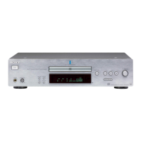
77
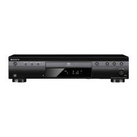
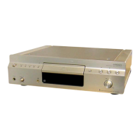
SCD-CE595
SCD-CE595
SECTION 4
DIAGRAMS
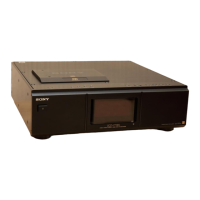
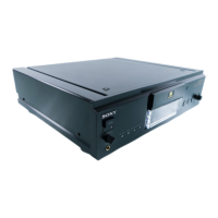
• Circuit Boards Location
NOTE FOR PRINTED WIRING BOARDS AND SCHEMATIC DIAGRAMS
Note on Printed Wiring Board:
• X : parts extracted from the component side.
• Y : parts extracted from the conductor side.
• W : indicates side identified with part number.
• f : internal component.
• : Pattern from the side which enables seeing.
C
B
These are omitted.
E
Q
Note Schematic Diagrams.
• All capacitors are in µF unless otherwise noted. (p: pF)
50 WV or less are not indicated except for electrolytics and
tantalums.
• All resistors are in Ω and
1
/
4
W or less unless otherwise
specified.
• f : internal component.
• C : panel designation.
• A : B+ Line.
• B : B– Line.
•Voltages and waveforms are dc with respect to ground
under no-signal conditions.
no mark: SACD PLAY
( ) : CD PLAY
•Voltages are taken with a VOM (Input impedance 10 MΩ).
Voltage variations may be noted due to normal production
tolerances.
•Waveforms are taken with a oscilloscope.
Voltage variations may be noted due to normal production
tolerances.
• Circled numbers refer to waveforms.
• Signal path.
J : CD
c : CD DIGITAL OUT (OPTICAL)
Caution:
Pattern face side: Parts on the pattern face side seen from
(Side B) the pattern face are indicated.
Parts face side: Parts on the parts face side seen from
(Side A) the parts face are indicated.
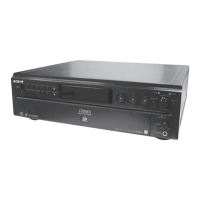
1.4 Vp-p
1 IC001 tl SIGO (CD)
1.4 Vp-p
1
IC001 tl SIGO (SACD)
200 ns/DIV
40 ns/DIV
•Waveforms
• Indication of transistor.
– RF Board – – MAIN Board – – DISPLAY Board –
4 IC320 2,4,6,q;,qs
1.4 Vp-p
3
IC706
<z./ RF IN (SACD)
2
IC706 uk DSPHREFO
354 ns
3.5 Vp-p
40 ns/DIV
3.3 to 3.5
Vp-p
88.6 ns
5 IC801 3 X1
200 ns
3.1 Vp-p
1 V/DIV, 200 ns/DIV
Note:
The components identi-
fied by mark 0 or dot-
ted line with mark 0 are
critical for safety.
Replace only with part
number specified.
Note:
Les composants identifiés
par une marque 0 sont cri-
tiques pour la sécurité.
Ne les remplacer que par une
piéce portant le numéro
spécifié.
MAIN boar