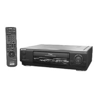
SLV-478/677HF/678HF/688HF/L47/L48/L57/
L58/L67HF/L68HF/L77HF/L78HF/X50/X60HF
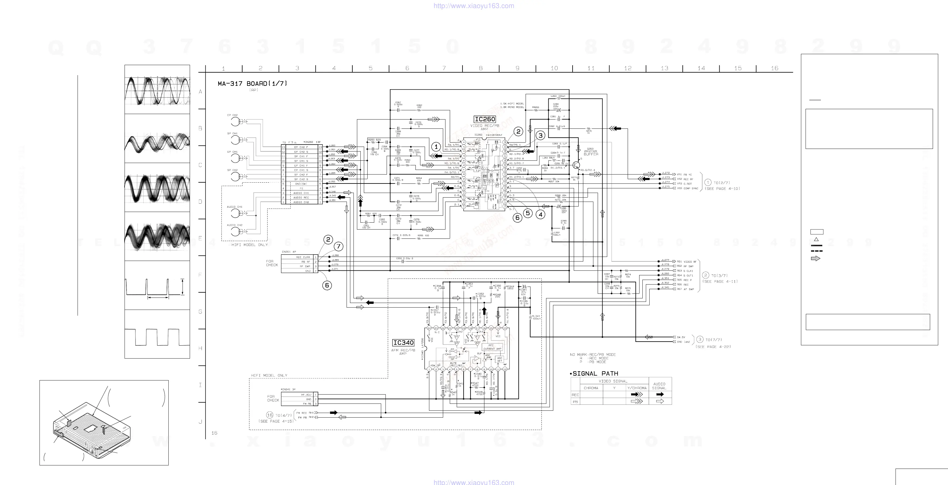
MA-317 (REC/PB AMP) SCHEMATIC DIAGRAM
— Ref. No.: MA-317 board; 1,000 series —
4-5 4-6 4-7
REC/PB AMP
MA-317 (1/7)
• See page 4-3 for MA-317 BOARD printed wiring board.
IF702
DS-79
(OPERATION SWITCHES)
JK-161
(LINE IN 2)
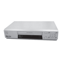
SLV-688HF/L57/L58/
L77HF/L78HF/X50
MA-317
REC/PB AMP, VIDEO,
SERVO/SYSTEM CONTROL,
AUDIO, MODE CONTROL,
TUNER, POWER SUPPLY
ACE ASSEMBLY
MA-317
BOARD
(1/3)
1
IC260 4 REC
2
IC260 #º REC
CN261 1 REC
3
IC260 @• REC
20mV/Div
0.1µsec/div
0.5V/Div
0.1µsec/div
1V/Div
0.1µsec/div
4
IC260 @™ PB
200mV/Div
0.1µsec/div
5
IC260 !• REC/PB
2.3Vp-p
H
6
IC260 !¶ REC/PB
CN261 3 REC/PB
5Vp-p
30Hz
MA-317 BOARD
CJ570 A-4
CN101 C-9
CN102 E-3
CN103 I-6
CN161 I-13
CN260 B-10
CN261 B-9
CN301 B-6
CN302 B-6
CN341 B-12
CN401 J-2
CN423 D-12
CN600 B-1
CNJ980 A-3
D103 G-7
D109 E-8
D161 H-3
D162 H-3
D382 A-12
D383 A-12
D405 J-13
D501 B-4
D560 B-4
D600 C-1
D601 D-3
D602 E-2
D603 D-2
D604 D-2
D605 E-1
D606 G-1
D607 F-1
D608 F-2
D609 F-2
D610 G-2
D611 F-12
D612 F-12
D616 D-2
D702 C-13
D980 A-4
D981 A-4
D982 B-4
IC101 I-4
IC160 I-10
IC161 G-7
IC162 H-7
IC201 D-6
IC202 E-5
IC260 B-10
IC301 C-6
IC340 B-11
IC360 D-10
IC403 J-10
IC420 J-8
IC501 C-3
IC601 H-12
IC602 F-1
IC733 H-13
IC980 B-4
PH101 H-9
PH102 H-6
PH600 E-1
Q101 F-3
Q102 F-11
Q103 G-8
Q201 B-6
Q202 C-6
Q208 C-5
Q209 D-5
Q210 E-6
Q211 E-6
Q260 B-9
Q301 C-7
Q331 C-8
Q387 A-12
Q401 J-13
Q501 C-4
Q502 D-4
Q560 B-5
Q601 D-2
Q602 C-1
Q603 E-12
Q604 I-1
Q605 H-1
• For printed wiring boards.
• : Pattern from the side which enables seeing.
Caution :
Pattern face side: Parts on the pattern face side
(Conductor Side) seen from the pattern face are
indicated.
Pattern face side: parts on the parts face side seen
(Component Side) from the parts face are indicated.
• For schematic diagrams.
• Caution when replacing chip parts.
New parts must be attached after removal of chip.
Be careful not to heat the minus side of tantalum
capacitor, because it is damaged by the heat.
• All resistor are in ohms, 1/4W unless otherwise noted.
Chip resistor are 1/10W unless otherwise noted.
kΩ: 1000Ω, MΩ, : 1000kΩ.
• All capacitors are in µF unless otherwise noted. pF : µ
µF. 50V or less are not indicated except for electrolytics
and tantalums.
• : panel designation.
•
: internal component.
•
: B+ Line. *
•
: B– Line. *
•
: IN/OUT direction of (+,–) B LINE. *
• Circled numbers refer to waveforms. *
• Readings are taken with a color-bar signal input.
• Voltage are dc between ground and measurement
points.*
• Readings are taken with a digital multimeter (DC10MΩ).*
• Voltage variations may be noted due to normal production
tolerances.*
When indicating parts by reference number, please
include the board name.
• * : indicated by the color red.
THIS NOTE IS COMMON FOR PRINTED WIRING
BOARDS AND SCHEMATIC DIAGRAMS.
(In addition to this, the necessary note is
printed in each block.)
w
w
w
.
x
i
a
o
y
u
1
6
3
.
c
o
m
Q
Q
3
7
6
3
1
5
1
5
0
9
9
2
8
9
4
2
9
8
T
E
L
1
3
9
4
2
2
9
6
5
1
3
9
9
2
8
9
4
2
9
8
0
5
1
5
1
3
6
7
3
Q
Q
TEL 13942296513 QQ 376315150 892498299
TEL 13942296513 QQ 376315150 892498299
http://www.xiaoyu163.com
http://www.xiaoyu163.com