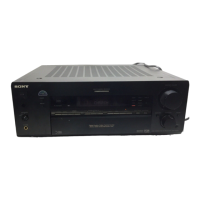
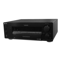
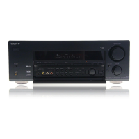
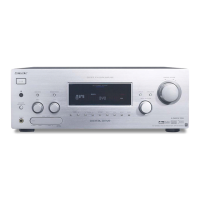
STR-DB900
2
Unleaded solder
Boards requiring use of unleaded solder are printed with the lead-
free mark (LF) indicating the solder contains no lead.
(Caution: Some printed circuit boards may not come printed with
the lead free mark due to their particular size.)
: LEAD FREE MARK
Unleaded solder has the following characteristics.
• Unleaded solder melts at a temperature about 40°C higher than
ordinary solder.
Ordinary soldering irons can be used but the iron tip has to be
applied to the solder joint for a slightly longer time.
Soldering irons using a temperature regulator should be set to
about 350°C.
Caution: The printed pattern (copper foil) may peel away if the
heated tip is applied for too long, so be careful!
SAFETY-RELATED COMPONENT WARNING!!
COMPONENTS IDENTIFIED BY MARK 0 OR DOTTED LINE
WITH MARK 0 ON THE SCHEMATIC DIAGRAMS AND IN THE
PARTS LIST ARE CRITICAL TO SAFE OPERATION. REPLACE
THESE COMPONENTS WITH SONY PARTS WHOSE PART NUM-
BERS APPEAR AS SHOWN IN THIS MANUAL OR IN SUPPLE-
MENTS PUBLISHED BY SONY.
• Strong viscosity
Unleaded solder is more viscous (sticky, less prone to flow)
than ordinary solder so use caution not to let solder bridges
occur such as on IC pins, etc.
• Usable with ordinary solder
It is best to use only unleaded solder but unleaded solder may
also be added to ordinary solder.
Notes on chip component replacement
• Never reuse a disconnected chip component.
• Notice that the minus side of a tantalum capacitor may be dam-
aged by heat.
TABLE OF CONTENTS
1. SERVICING NOTES
1-1. AMP Board, DIGITAL Board Service Position .............. 3
1-2. Note on Checking AMP Board or DIGITAL Board
While Turning on Electricity ........................................... 3
1-3. Note on AMP Board Removal......................................... 4
1-4. Note on Heat Sink Installation ........................................ 4
1-5. Note on Checking POWER Board While Turning on
Electricity 1 ..................................................................... 5
1-6. Note on Checking POWER Board While Turning on
Electricity 2 ..................................................................... 5
2. GENERAL ................................................................... 6
3. TEST MODE ............................................................... 7
4. DIAGRAMS
4-1. Block Diagram — INPUT/TUNER Section — ............. 13
4-2. Block Diagram — AUDIO DSP Section —................... 14
4-3. Block Diagram — DAMP Section — ............................ 15
4-4. Block Diagram — DISPLAY Section — ....................... 16
4-5. Schematic Diagram — DIGITAL Section (1/3) — ........ 17
4-6. Schematic Diagram — DIGITAL Section (2/3) — ........ 18
4-7. Schematic Diagram — DIGITAL Section (3/3) — ........ 19
4-8. Printed Wiring Board — DIGITAL Board (Side A) —.. 20
4-9. Printed Wiring Board — DIGITAL Board (Side B) —.. 21
4-10. Printed Wiring Board — AMP Board (Side A) — ......... 22
4-11. Printed Wiring Board — AMP Board (Side B) — ......... 23
4-12. Schematic Diagram — AMP Board (1/4) — ................. 24
4-13. Schematic Diagram — AMP Board (2/4) — ................. 25
4-14. Schematic Diagram — AMP Board (3/4) — ................. 26
4-14. Schematic Diagram — AMP Board (4/4) — ................. 27
4-15. Printed Wiring Board
— VIDEO, ANALOG IN Board — ................................ 28
4-16. Schematic Diagram
— VIDEO, ANALOG IN Board — ................................ 29
4-17. Printed Wiring Board — DISPLAY Section — ............. 30
4-18. Schematic Diagram — DISPLAY Section — ................ 31
4-19. Printed Wiring Board — POWER Section — ................ 32
4-20. Schematic Diagram — POWER Section — .................. 33
5. EXPLODED VIEWS
5-1. Case Section .................................................................... 43
5-2. Front Panel Section ......................................................... 44
5-3. Chassis Section ................................................................ 45
6. ELECTRICAL PARTS LIST .................................. 46