37
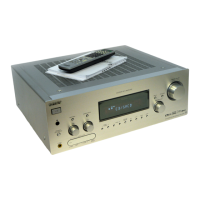
STR-DB900
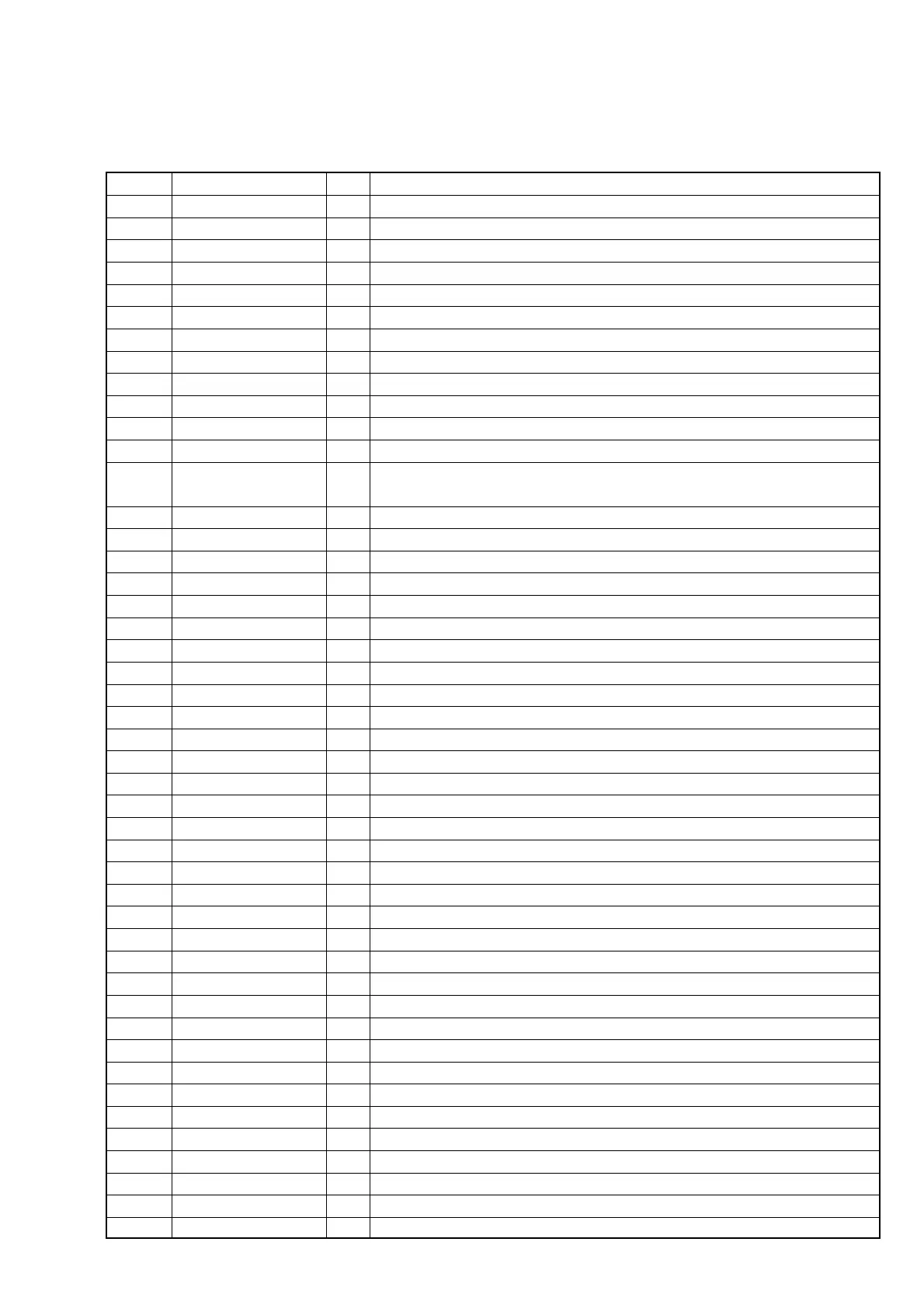
• IC Pin Function Description
DIGITAL BOARD IC206 CXD9718Q (AUDIO DSP)
Pin No. Pin Name I/O Description
1 VSS — Ground
2 XRST I System reset signal input
3 EXTIN I Not used. (Connected to ground.)
4 LRCKI3 I Not used. (Connected to ground.)
5VDDI — Power supply (+2.5 V)
6 BCKI3 I Not used. (Connected to ground.)
7 PLOCK O Not used. (Open)
8 VSS — Ground
9 MCLK1 I System clock input (13.5 MHz)
10 VDDI — Power supply (+2.5 V)
11 VSS — Ground
12 MCLK2 O System clock output (13.5 MHz)
13 MS I
Master/slave setting pin (“L”: internal clock, “H”: external clock)
Connected to ground.
14 SCKOUT O Internal system clock output
15 LRCKI1 I L/R sampling clock signal input from LC89056W
16 VDDE — Power supply (+3.3 V)
17 BCKI1 I Bit clock signal input from LC89056W
18 SDI1 I Audio serial data input
19 LRCKO O L/R sampling clock signal output to digital amp
20 BCKO O Bit clock signal output to digital amp
21 VSS — Ground
22 KFSIO I Audio clock signal input from LC89056W
23 to 26 SDO1 to SDO4 O Audio serial data output to digital amp
27 SPDIF O Not used. (Open)
28 LRCKI2 I L/R sampling clock signal input from LC89056W
29 BCKI2 I Bit clock signal input from LC89056W
30 SDI2 I Audio serial data input from analog audio and digital audio
31 VSS — Ground
32 HACN O Acknowledge signal output to MB91354APMT
33 HDIN I Serial data input from MB91354APMT
34 HCLK I Serial data transfer clock input from MB91354APMT
35 HDOUT O Serial data output to MB91354APMT
36 HCS I Chip select input from MB91354APMT
37 GP12 I GP data signal input from MB91354APMT
38 GP13 — Not used. (Open)
39 GP14 — Not used. (Open)
40 VDDI — Power supply (+2.5 V)
41 VSS — Ground
42 GP15 I/O Not used. (Open)
43 OE0 O Not used. (Open)
44 CS0 O Chip select signal output to DRAM
45 WE0 O Write enable signal output to DRAM
46 VDDE — Power supply (+3.3 V)
47 WMD1 I Not used. (Connected to VDD.)
48 VSS — Ground
49 WMD0 I Not used. (Connected to VDD.)