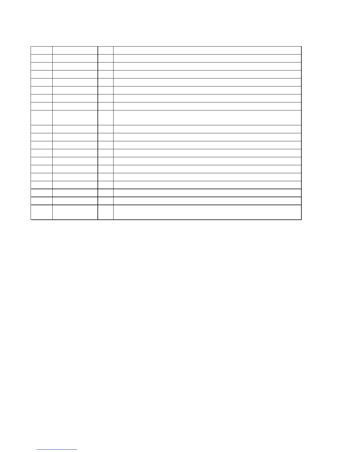
52
Pin No. Pin Name I/O Description
99
CLKI I
Master clock signal input terminal (10MHz)
100
CLKO O
Master clock signal output terminal (10MHz)
101
VSS1 —
Ground terminal
102
VDD0 —
Power supply terminal (+3.3V)
103
AVSS —
Ground terminal (for PLL cell)
104
AVDD —
Power supply terminal (+3.3V) (for PLL cell)
105
PLLCK I/O
PLL output/test clock signal input terminal (for check)
106
XPLLEN I
PLL cell oscillation enable signal input terminal “L”: oscillation enable
(fixed at “L” in this set)
107
TST I
Test data input terminal (Normally: fixed at “L”)
108
LRCT I
Frequency counter input terminal (fixed at “L” in this set)
109
LROUT O
Clock driver signal output terminal (for check)
110
BKOUT O
Clock driver signal output terminal (for check)
111
VSS2 —
Ground terminal
112
VDD1 —
Power supply terminal (+3.3V)
113
BCK0 I
Clock 0 signal input from the digital audio interface receiver (IC1101)
114
BCK1 I
Clock 1 signal input from the digital audio interface receiver (IC1101)
115
LRCK0 I
Clock 0 signal input from the digital audio interface receiver (IC1101)
116
LRCK1 I
Clock 1 signal input from the digital audio interface receiver (IC1101)
117 to
120
SIA to SID —
Serial data input from the dolby digital audio decoder (IC1301)