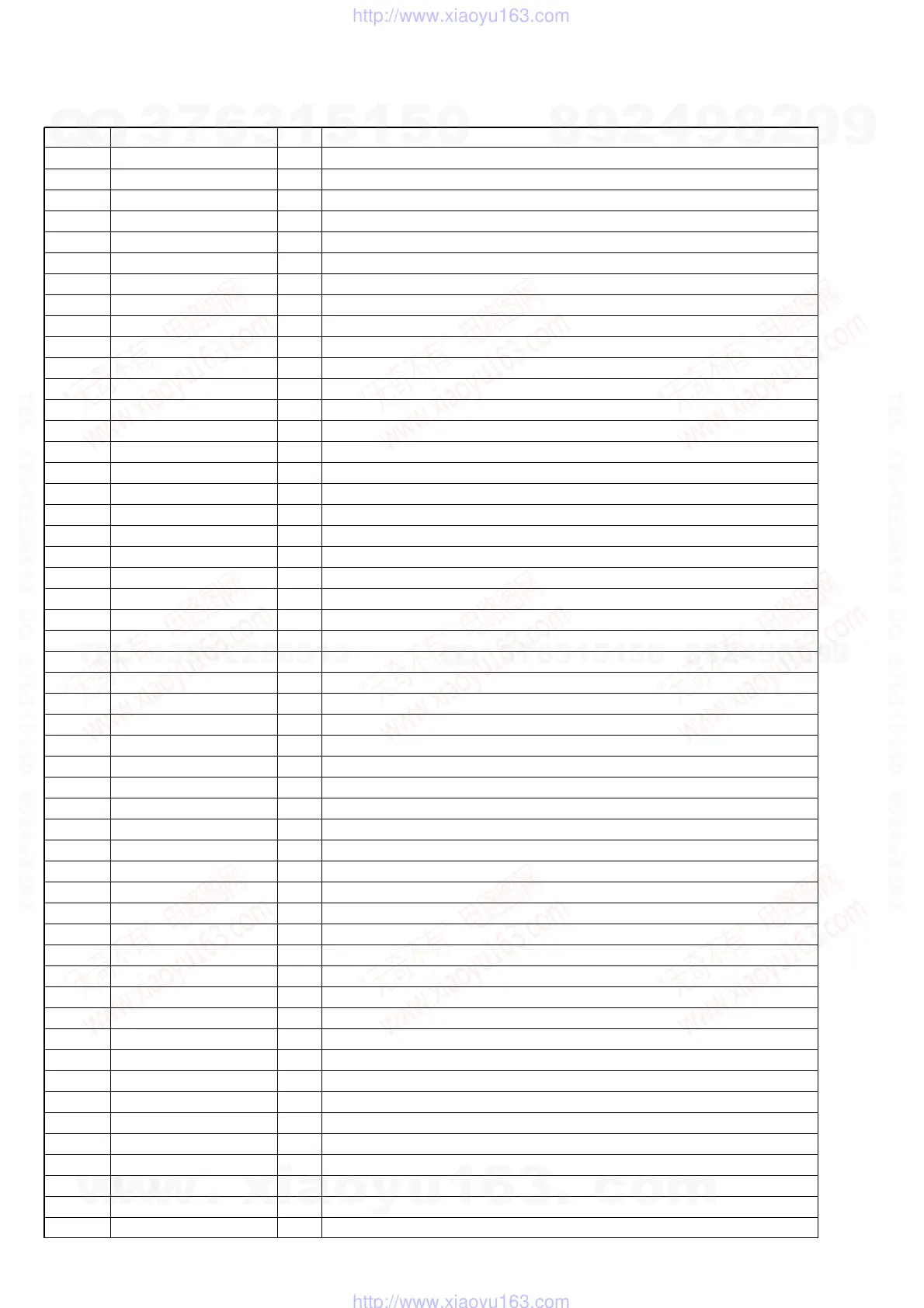
70
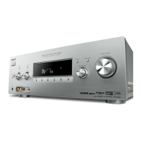
STR-DG910
IC3513 SII9030CTU-7 (HDMI TX) (HDMI RE BOARD (2/4))
Pin No. Pin Name I/O Pin Description
1 HSYNC I Horizontal synchronize signal input from HDMI RX.
2 VSYNC I Vertical synchronize signal input from HDMI RX.
3 CGND — Ground
4 CVCC18 — Power supply terminal (+1.8 V)
5 SPDIF I SPDIF signal input from HDMI RX.
6MCLK I Audio master clock signal input from HDMI RX.
7 to 10 SD3 to SD0 I Serial data input from HDMI RX.
11 WS I Word select signal input from HDMI RX.
12 SCK I Serial clock signal input from HDMI RX.
13 IOVCC — Power supply terminal (+3.3 V)
14 IOGND — Ground
15 CGND — Ground
16 CVCC18 — Power supply terminal (+1.8 V)
17 INT O Interrupt signal output for HDMI controller.
18 HPD I Hot plug detect signal input from HDMI OUT connector.
19 DSDA I/O I2C two-way data bus with HDMI OUT connector.
20 DSCL O I2C clock signal output for HDMI OUT connector.
21 RSVDL — Not used. (Fixed at L)
22 PGND1 — Ground
23 PVCC1 — Power supply terminal (+3.3 V)
24 EXT_SWING — Not used. (Fixed at H)
25 AGND — Ground
26 TXC– O TMDS clock signal output for HDMI OUT connector.
27 TXC+ O TMDS clock signal output for HDMI OUT connector.
28 AVCC — Power supply terminal (+3.3 V)
29 TX0– O TMDS data output 0 for HDMI OUT connector.
30 TX0+ O TMDS data output 0 for HDMI OUT connector.
31 AGND — Ground
32 TX1– O TMDS data output 1 for HDMI OUT connector.
33 TX1+ O TMDS data output 1 for HDMI OUT connector.
34 AVCC — Power supply terminal (+3.3 V)
35 TX1– O TMDS data output 2 for HDMI OUT connector.
36 TX1+ O TMDS data output 2 for HDMI OUT connector.
37 AGND — Ground
38 PVCC2 — Power supply terminal (+3.3 V)
39 PGND2 — Ground
40 NC — Not used. (Open)
41 CI2CA — Not used. (Fixed at L)
42 RESET I Reset signal input from HDMI controller. (L: Reset)
43 CSCL I I2C clock signal input from HDMI controller.
44 CSDA I/O I2C two-way data bus with HDMI section.
45 CVCC18 — Power supply terminal (+1.8 V)
46 CGND — Ground
47 IOGND — Ground
48 IOVCC — Power supply terminal (+3.3 V)
49 to 58 D23 to D14 I Serial data input 23 to 14 from HDMI RX and video processor.
59 CVCC18 — Power supply terminal (+1.8 V)
60 CGND — Ground
61 to 65 D13 to D9 I Serial data input 13 to 9 from HDMI RX and video processor.
66 IDCK I Output data clock signal input from HDMI RX.
67 to 70 D8 to D5 I Serial data input 8 to 5 from HDMI RX and video processor.
71 IOVCC — Power supply terminal (+3.3 V)
w
w
w
.
x
i
a
o
y
u
1
6
3
.
c
o
m
Q
Q
3
7
6
3
1
5
1
5
0
9
9
2
8
9
4
2
9
8
T
E
L
1
3
9
4
2
2
9
6
5
1
3
9
9
2
8
9
4
2
9
8
0
5
1
5
1
3
6
7
3
Q
Q
TEL 13942296513 QQ 376315150 892498299
TEL 13942296513 QQ 376315150 892498299
http://www.xiaoyu163.com
http://www.xiaoyu163.com