4
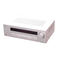
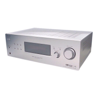
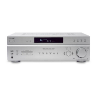
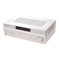
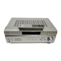
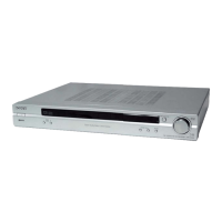
STR-K650P
TABLE OF CONTENTS
1. GENERAL ·········································································· 5
2. TEST MODE ······································································ 6
3. DIAGRAMS ········································································ 7
3-1. Circuit Board Location················································· 7
3-2. Block Diagrams – MAIN Section – ····························· 8
– DISPLAY/POWER Section – ··································· 9
3-3. Printed Wiring Board – DIGITAL Board (SIDE A) – 10
3-4. Printed Wiring Board – DIGITAL Board (SIDE B) – 11
3-5. Schematic Diagram – DIGITAL Section (1/2) – ······· 12
3-6. Schematic Diagram – DIGITAL Section (2/2) – ······· 13
3-7. Printed Wiring Board – MAIN Board – ····················· 14
3-8. Schematic Diagram – MAIN Section (1/3) –············· 15
3-9. Schematic Diagram – MAIN Section (2/3) –············· 16
3-10. Schematic Diagram – MAIN Section (3/3) –············· 17
3-11. Printed Wiring Board – POWER Section – ··············· 18
3-12. Printed Wiring Board – DISPLAY Board – ··············· 19
3-13. Schematic Diagram – DISPLAY Section –················ 20
3-14. Printed Wiring Board – VIDEO Section – ················· 21
3-15. Schematic Diagram – VIDEO Board – ······················ 22
3-16. IC Block Diagrams····················································· 23
3-17. IC Pin Function Descriptions ····································· 25
4. EXPLODED VIEWS ······················································ 27
4-1. Front Panel Section ····················································· 27
4-2. Chassis Section ··························································· 28
5. ELECTRICAL PARTS LIST ······································· 29