1111
STR-K660P
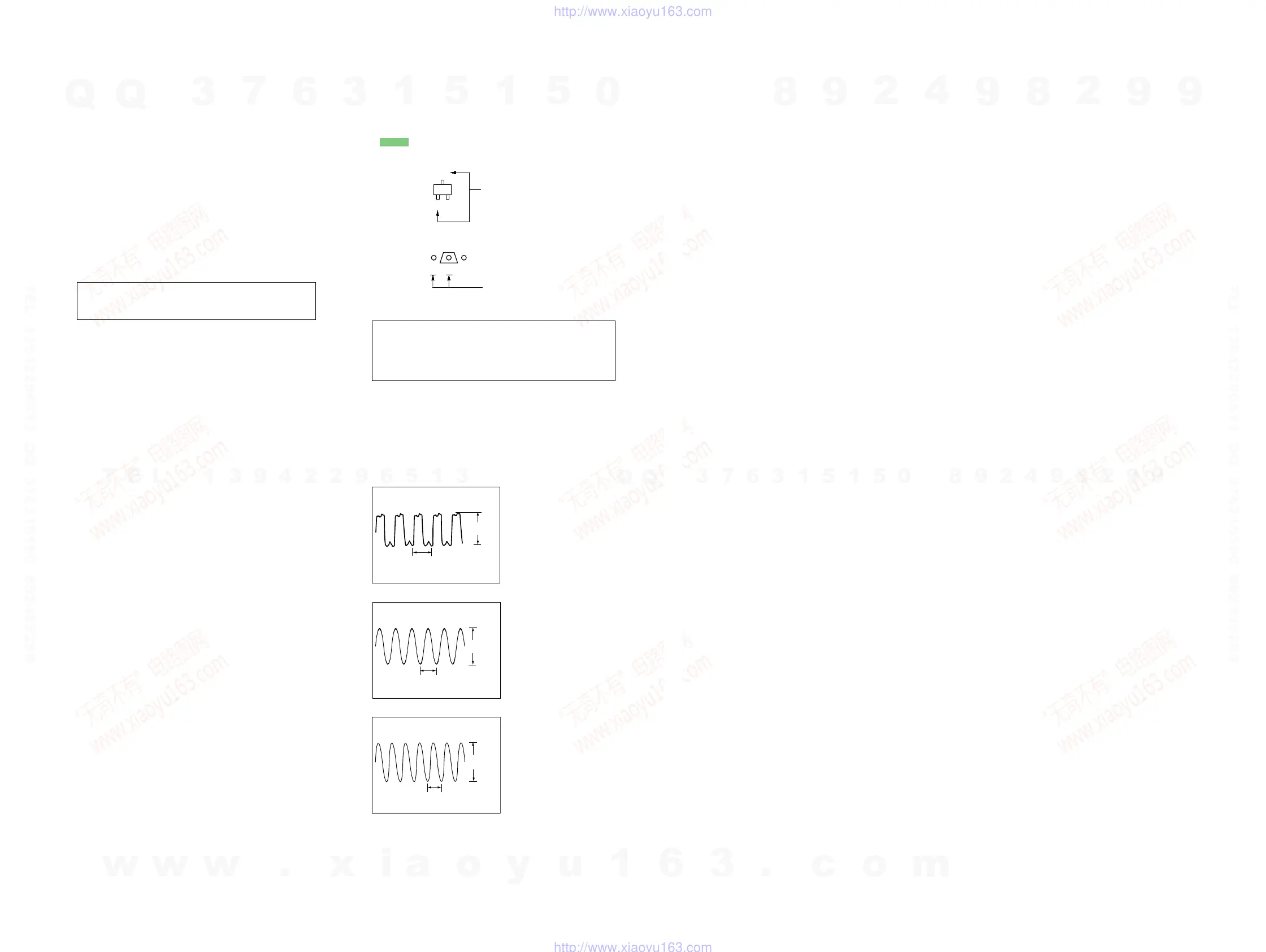
• Waveforms
DIGITAL Board
For schematic diagrams.
Note:
• All capacitors are in µF unless otherwise noted. p : µµF
50 WV or less are not indicated except for electrolytics
and tantalums.
• All resistors are in Ω and
1
/
4
W or less unless otherwise
specified.
•%: indicates tolerance.
•
f
: internal component.
• 2 : nonflammable resistor.
• 5 : fusible resistor.
• C : panel designation.
• A : B+ Line.
• B : B– Line.
•Voltages and waveforms are dc with respect to ground
under no-signal (detuned) conditions.
No mark : FM
•Voltages are taken with a VOM (Input impedance 10 MΩ).
Voltage variations may be noted due to normal produc-
tion tolerances.
•Waveforms are taken with a oscilloscope.
• Circled numbers refer to waveforms.
• Signal path.
F : FM
J : ANALOG INPUT
c : DIGITAL INPUT
•Abbreviation
E51 : Chilean and Peruvian models
MX : Mexican model
SP : Singapore model
THIS NOTE IS COMMON FOR PRINTED WIRING
BOARDS AND SCHEMATIC DIAGRAMS.
(In addition to this necessary note is printed in each
block.)
Caution:
Pattern face side: Parts on the pattern face side seen from
(Side A) the pattern face are indicated.
Parts face side: Parts on the parts face side seen from
(Side B) the parts face are indicated.
For printed wiring boards.
Note:
• X : parts extracted from the component side.
•
a
: Through hole.
•
f
: internal component.
• : Pattern from the side which enables seeing.
C
B
These are omitted.
E
Q
B
These are omitted.
CE
1 IC1101 wa (XOUT)
4.7 Vp-p
1V/div, 40ns/DIV
81.4ns
(12.288MHz)
2 IC1201 9 (MCLK1)
2.8 Vp-p
73.6ns (13.59MHz)
1V/div, 40ns/DIV
3 IC1601 id (XI)
3.5Vp-p
62.5ns (16MHz)
1V/div, 40ns/DIV
Note: The components identified by mark 0 or dotted line
with mark 0 are critical for safety.
Replace only with part number specified.
w
w
w
.
x
i
a
o
y
u
1
6
3
.
c
o
m
Q
Q
3
7
6
3
1
5
1
5
0
9
9
2
8
9
4
2
9
8
T
E
L
1
3
9
4
2
2
9
6
5
1
3
9
9
2
8
9
4
2
9
8
0
5
1
5
1
3
6
7
3
Q
Q
TEL 13942296513 QQ 376315150 892498299
TEL 13942296513 QQ 376315150 892498299
http://www.xiaoyu163.com
http://www.xiaoyu163.com