– 7 – – 8 –
SECTION 4
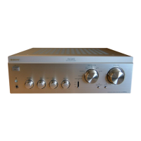
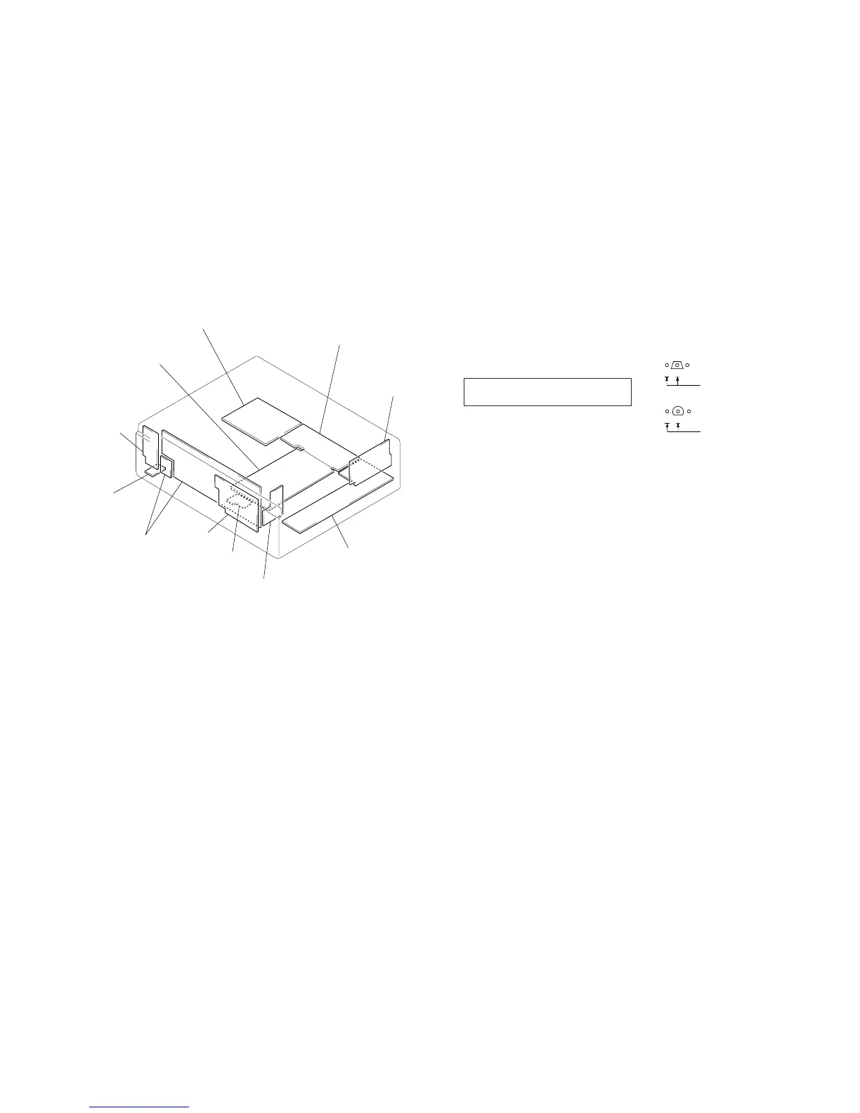
DIAGRAMS
• Circuit Boards Location
4-1. NOTE FOR PRINTED WIRING BOARDS AND SCHEMATIC DIAGRAMS
(In addition to this, the necessary note is printed in each block.)
Note on Schematic Diagram:
• All capacitors are in µF unless otherwise noted. pF: µµF
50 WV or less are not indicated except for electrolytics
and tantalums.
• All resistors are in Ω and
1
/
4
W or less unless otherwise
specified.
• 2 : nonflammable resistor.
• 5 : fusible resistor.
• C : panel designation.
Note on Printed Wiring Boards:
• X : parts extracted from the component side.
• b : Pattern from the side which enables seeing.
• Indication of transistor.
• U : B+ Line.
• V : B– Line.
• H : adjustment for repair.
• Voltages and waveforms are dc with respect to ground
under no-signal conditions.
no mark: POWER ON
• Voltages are taken with a VOM (Input impedance 10 MΩ).
Voltage variations may be noted due to normal produc-
tion tolerances.
• Waveforms are taken with a oscilloscope.
Voltage variations may be noted due to normal produc-
tion tolerances.
• Circled numbers refer to waveforms.
• Signal path.
K: TUNER
NOTE:The components identified by mark ! or dotted line
with mark ! are critical for safety.
Replace only with part number specified.
B
These are omitted.
CE
Q
B
These are omitted.
CE
Q
SP TM board
PS board
MAIN board
PHONO board
INPUT board
VOL board
SW board
LED board
PANEL board
HP board
POWER LED board