– 33 –
KV-BM142M70
RM-W101
4-3. SCHEMATIC DIAGRAM INFORMATION
Note:
• All capacitors are in µF unless otherwise noted.
• All electrolytic capacitors are rated at 50V unless otherwise
noted.
• All resistors are in ohms.
kΩ = 1000Ω, MΩ = 1000kΩ
• Indication of resistance which does not have rating
electrical power is as follows.
Pitch: 5 mm
Rating electrical power 1/4W (CHIP: 1/10W)
• : nonflammable resistor.
• : fusible resistor.
• f : internal component.
• : panel designation or adjustment for repair.
• All variable and adjustable resistors have characteristic
curve B unless otherwise noted.
• Readings are taken with a color-bar signal input.
no mark : Common
( ) : PAL
[ ] : NTSC 3.58
• Readings are taken with a 10 MΩ digital multimeter.
• Voltage are dc with respect to ground unless otherwise
noted.
• Voltage variations may be noted due to normal
production tolerances.
• All voltage are in Volt.
• ✽ : Cannot be measured.
• Circled numbers are waveform references.
• : B +bus.
• : B –bus.
• k : signal path.
Note: The reference number which starts with Wxxx
(eg: W003) indicates a wire to wire connection.
Note: Components marked as XX are not fitted on this
model.
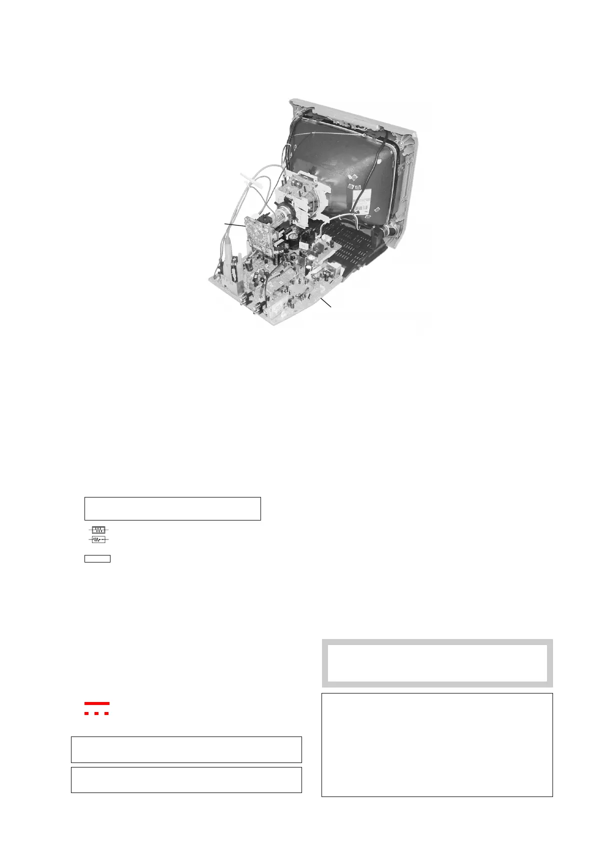
A board
C board
4-2. CIRCUIT BOARDS LOCATION
Reference information
RESISTOR : RN METAL FILM
: RC SOLID
: FPRD NONFLAMMABLE CARBON
: FUSE NONFLAMMABLE FUSIBLE
: RS NONFLAMMABLE METAL
OXIDE
: RB NONFLAMMABLE CEMENT
: RW NONFLAMMABLE
WIREWOUND
: ✽ ADJUSTMENT RESISTOR
COIL : LF-8L MICRO INDUCTOR
CAPACITOR : TA TANTALUM
: PS STYROL
: PP POLYPROPYLENE
: PT MYLAR
: MPS METALIZED POLYESTER
: MPP METALIZED POLYPROPYLENE
: ALB BIPOLAR
: ALT HIGH TEMPERATURE
: ALR HIGH RIPPLE
Note: The component identified by shading and
mark ! are critical for safety. Replace only
with part number specified.
Note: “A” board schematic diagram is divided into 7 blocks.
Each block is named by its function and block
“number”. eg: Processor (Block 001)
Joint connection between boards can be identified
using the block number followed by the grid's guide.
eg: -<PWR-OFF-MUTE
002 : 4E
Meaning: Block 001 joint "PWR-OFF MUTE" is
connected to Block 002 joint "PWR-OFF MUTE"
located at grid 4E.