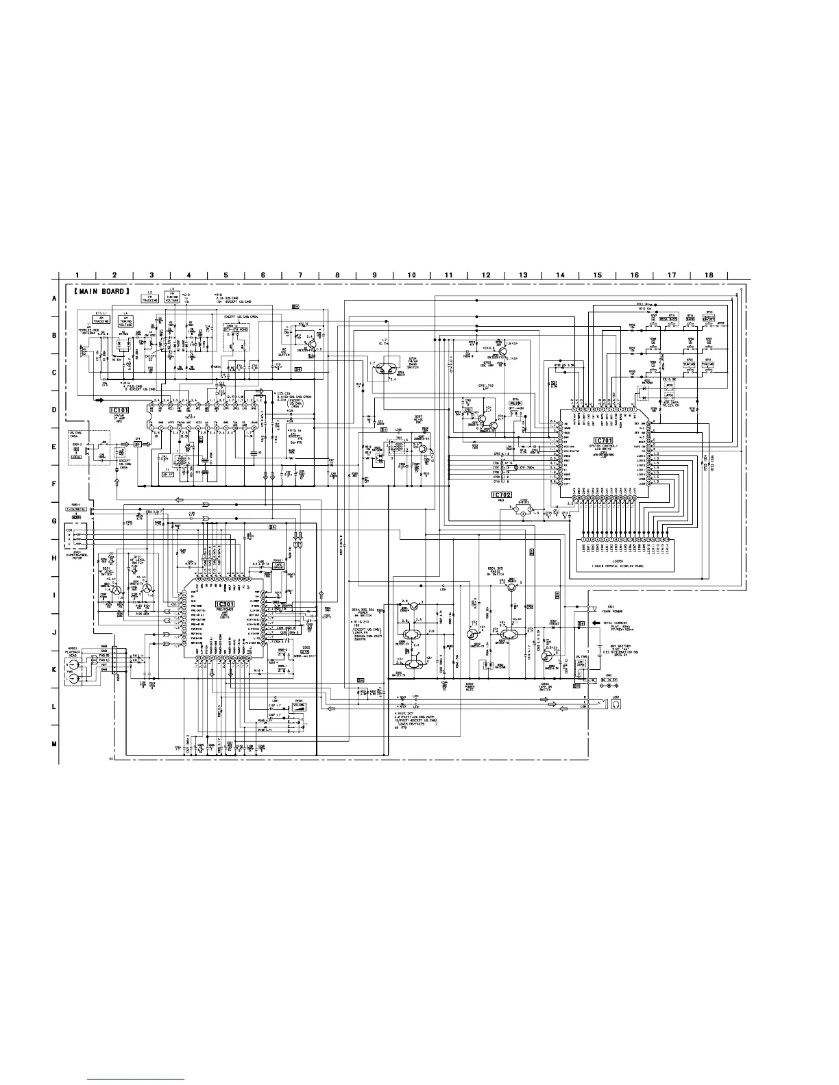
(EE)
(EXCEPT EE)
– 15 – – 16 –
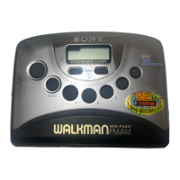
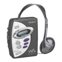
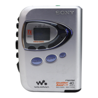
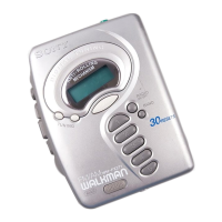
WM-FX271/FX275
Note:
• All capacitors are in µF unless otherwise noted.
pF: µµF 50 WV or less are not indicated except
for electrolytics and tantalums.
• All resistors are in Ω and
1
/
4
W or less unless
otherwise specified.
• % : indicates tolerance.
•
¢
: internal component.
• C : panel designation.
5-4. SCHEMATIC DIAGRAM • Refer to page 17 for IC Block Diagrams.
• U : B+ Line.
• H : adjustment for repair.
• Total current is measured with no cassette
installed.
• Power voltage is dc 3 V and fed with regulated
dc power supply from battery terminal.
• Voltage is dc with respect to ground under
no-signal (detuned) condition.
no mark : FM
( ) : AM
< > : PB
• Voltages are taken with a VOM (Input
impedance 10 MΩ).
Voltage variations may be noted due to normal
production tolerances.
• Signal path.
F : FM
f : AM
E : PB
• Abbreviation
CND : Canadian model
CEV : Poland, Czech, Greece and Turkey
model
CH : Chinese model
2AEP : Earphone (MDR-023) model
EE : East European model
FR : French model
C&SA : Central and South America model
9E : No indication of country of origin
E : Indication of country of origin
AEP : Headphone (MDR-E805LP) model
 Loading...