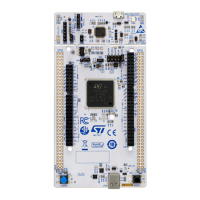
The main features of the Inventek system ISM43362-M3G-L44 module are:
• Based on the Broadcom BCM43362 MAC/Baseband/Radio device
• Supports Broadcom WICED SDK
• CPU Arm
®
Cortex
®
-M3 32-bit RISC core from STMicroelectronics
• IEEE 802.11n D7.0, OFDM-72.2 Mbps, single-stream width of 20 MHz, and short GI
• IEEE 802.11g, OFDM 54 Mbps
• IEEE 802.11b, DSSS 11 Mbps
• IEEE 802.11i, Security
– WPA (Wi‑Fi
®
Protected Access) –PSK/TKIP
– WPA2 (Wi‑Fi
®
Protected Access 2) –AES/CCMP/802.1x authentication
• GPIO, 5 ADC (SPI interface utilizes ADC pins)
• Power-saving mode allows the design of low-power applications
• Lead-free design which is compliant with ROHS requirements
• EMI/EMC Metal Shield for best RF performance in noisy environments and to accommodate for lower RF
emissions/signature for easier FCC compliance
• FCC/CE compliance certification
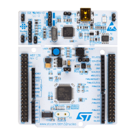
On MB1297 revision E, the firmware revision inside the Wi‑Fi
®
module must be C3.5.2.5.STM. The Wi‑Fi
®
module maximum output power is limited to 9 dBm to fulfill FCC/IC/CE requirements. A Wi‑Fi
®
output power
higher than 9 dBm at the Wi‑Fi
®
antenna is prohibited.
Note:
Since Wi
‑
Fi
®
and Bluetooth
®
Low Energy modules are using the same frequency ISM band (2.4 GHz to
2.485 GHz), the simultaneous activity of both modules may affect the RF performances of Wi
‑
Fi
®
or Bluetooth
®
Low Energy (in terms of range or throughput).
6.9.3 Dynamic NFC Tag based on ST25DV04K with its printed NFC antenna
The ST25DV04K device is an NFC RFID Tag offering 4 Kbit of electrically erasable programmable memory
(EEPROM). ST25DV04K offers two interfaces. The first one is an I
2
C serial link and can be operated from a DC
power supply. The second one is an RF-link activated when ST25DV04K acts as a contactless memory powered
by the received carrier electromagnetic wave.
In I
2
C mode, the ST25DV04K user memory contains up to 512 bytes which could be split into four flexible and
protectable areas. In RF mode, following ISO/IEC 15693 or NFC forum type 5 recommendations, ST25DV04K
user memory contains up to 128 blocks of 4 bytes which can be split into four flexible and protectable areas.
ST25DV04K offers a fast transfer mode between the RF and contact worlds, thanks to a 256-byte volatile buffer
(also called Mailbox). In addition, the GPO pin of the ST25DV04K provide data informing the contact world about
incoming events, like RF field detection, RF activity in progress or mailbox message availability. An energy
harvesting feature is also proposed when external conditions make it possible.
The main features of the ST25DV04K are:
I
2
C interface
•
Two-wire I
2
C serial interface supporting 1MHz protocol
• Single supply voltage from 1.8 V to 5.5 V
• Multiple bytes write programming, up to 256 bytes
Contactless interface
• Based on ISO/IEC 15693
• NFC Forum Type 5 tag certified by the NFC Forum
• Support of all ISO/IEC 15693 modulations, coding, sub-carrier modes, and data rates
• Custom fast read access up to 53 Kbps
• Single and multiple blocks read (same for extended commands)
• Single and multiple blocks write (up to 4) (same for extended commands)
• Internal tuning capacitance: 28.5 pF
UM2708
RF modules
UM2708 - Rev 1
page 19/43
 Loading...