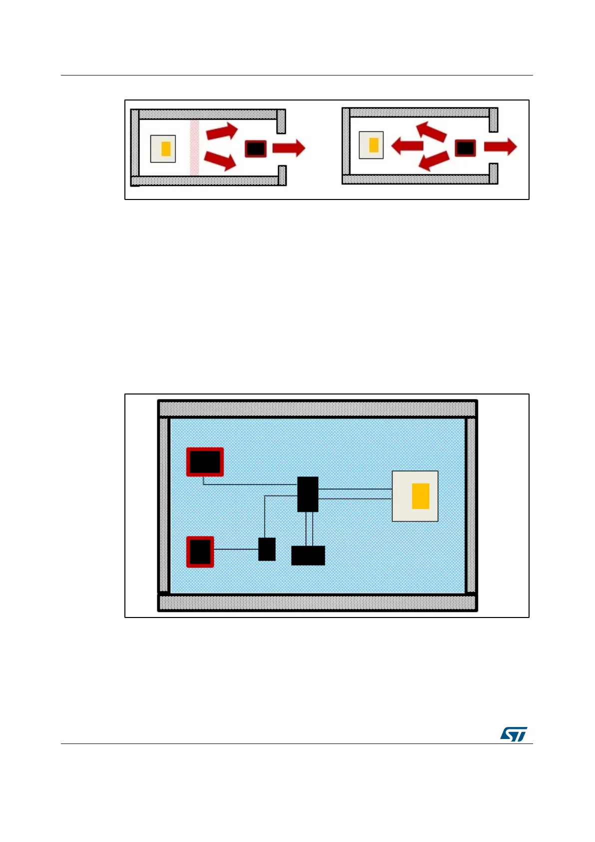
Figure 5: Top view of the sensor housing: on the left a correct design with the heat isolation,
on the right a wrong design
Heating conduction
Thermal conduction mostly occurs through the metal lines on the PCB and PCB itself.
In order to reduce this effect, we recommend adopting thin metal lines around the sensor,
at appropriate distance among the sensor and potential heat sources, avoiding metal areas
near and under the device.
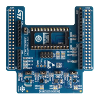
A good design rule is provided in Figure 6: "Sensor with a correct sensor placement on the
PCB to get the appropriate isolation from heat sources". As an example of good design, it
describes the positioning of the devices on the left, generating heat as far as possible from
the sensor, and in Figure 8: "Sensor wiring with wrong placement on the PCB" a wrong
layout with the devices generating heat too close to the sensor. In both cases thinner metal
lines are adopted.
Figure 6: Sensor with a correct sensor placement on the PCB to get the appropriate isolation
from heat sources