UM1681 Rev 3 15/23
UM1681 Hardware overview
22
2.6.4 Boot configuration
It is possible to reprogram microcontroller internal flash programming using Boot Assist
Mode (BAM) via SCI. The pins PA8 and PA9, (see Figure 12: User I/O pins PC4, PA8 and
PA9) have to be configured to enable the BAM functionality as following:
FABM (PA9) has to be connected to VDD_HV to enable serial boot (J13 jumper
closed).
ABS (PA8) has to be physically grounded to flash via SCI (J12 jumper closed).
If the BAM function is not used, these pins can be configured as normal I/O according to the
functions reported in the datasheet (see Section Appendix B: Reference documents).
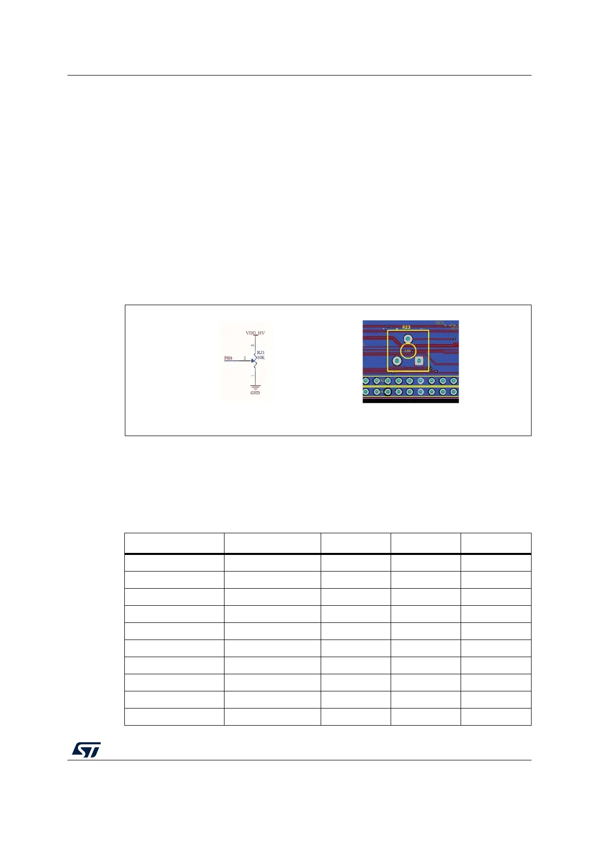
2.6.5 ADC input
A trimmer connected to the microcontroller PB8 input allows the user to check ADC. The
analog input voltage range is 0 V ÷ +V
DD_HV
.
Figure 13. Potentiometers (Schematic & PCB)
2.7 Daughter board connector and I/O headers
The I/O microcontroller pins are connected to a double 2x36 pin array (connectors X1-X2
and X3-X4).
Table 4. I/O headers
Pin number X1 X2 X3 X4
1 GND GND VBAT VBAT
2 PE[2] PE[3] GND GND
3PC[5]PC[4]TCKTDI
4 PE[4] PE[5] TDO TMS
5 PH[4] PH[5] PA[6] PA[5]
6 PH[6] PH[7] PC[2] PC[3]
7 PH[8] PE[6] PG[11] PG[10]
8 PE[7] PC[12] PE[15] PE[14]
9 PC[13] PB[1] PG[15] PG[14]
10 PB[2] PB[3] PE[12] PA[11]