Contents
1 Features...........................................................................2
2 Ordering information ..............................................................3
3 Development environment .........................................................4
3.1 System requirements ...........................................................4
3.2 Development toolchains .........................................................4
3.3 Firmware upgrade..............................................................4
4 Quick start ........................................................................5
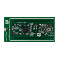
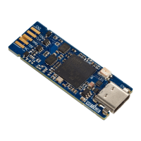
5 STLINK-V3MINIE functional description ............................................6
5.1 STLINK-V3MINIE overview ......................................................6
5.2 STLINK-V3MINIE frequency selection .............................................6
5.3 High‑performance modules ......................................................6
5.4 Hardware layout ...............................................................6
5.5 STLINK-V3MINIE functions ......................................................9
5.5.1 SWD with SWV ..........................................................9
5.5.2 JTAG..................................................................9
5.5.3 Virtual COM port (VCP)....................................................9
5.5.4 Mass-storage interface ....................................................9
5.5.5 LEDs..................................................................9
6 Board connectors ................................................................10
6.1 Connectors...................................................................10
6.2 Pads on board to CN2 BTB card edge connector...................................10
6.3 CN4 STDC14 connector........................................................11
7 Performance figures ..............................................................12
8 STLINK-V3MINIE board information ...............................................13
8.1 Product marking ..............................................................13
8.2 STLINK-V3MINIE product history ................................................13
8.2.1 Product identification LKV3MINIE$KT1.......................................13
8.3 Board revision history ..........................................................13
8.3.1 Board MB1762 revision B-01 ..............................................13
9 Federal Communications Commission (FCC) and Innovation, Science and Economic
Development Canada (ISED) Compliance Statements .............................14
9.1 FCC Compliance Statement ....................................................14
9.2 ISED Compliance Statement ....................................................14
Revision history .......................................................................15
UM2910
Contents
UM2910 - Rev 2
page 16/20
 Loading...