Hardware layout and configuration UM1570
22/41 UM1570 Rev 7
6.11 Solder bridges
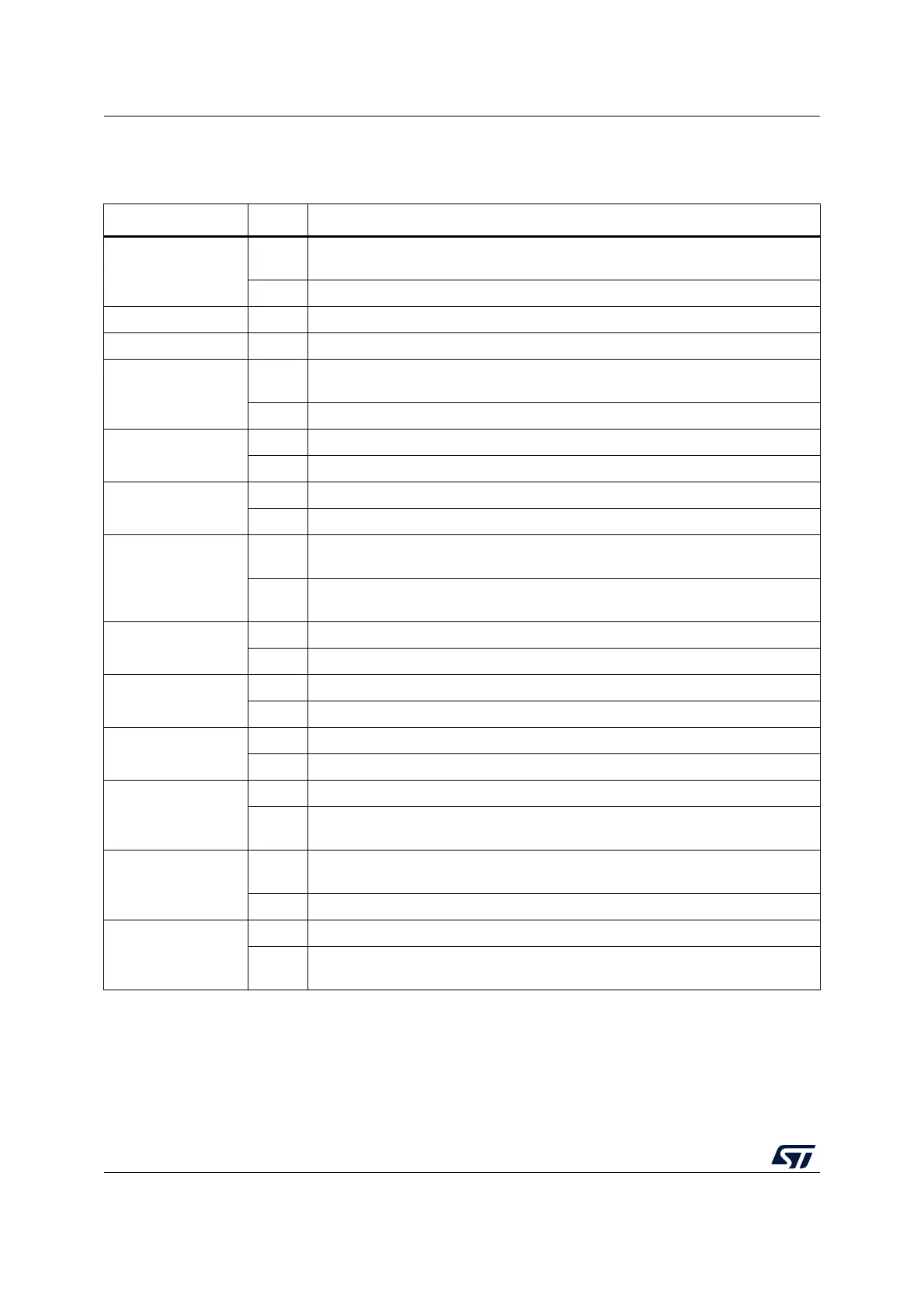
Table 6. Solder bridges
Bridge State
(1)
Description
SB17,18
(X1 crystal)
(2)
OFF
X1, C22, C23, R32, and R33 provide a clock. PF0 and PF1 are disconnected from
P2.
ON PF0 and PF1 are connected to P2 (R32 and R33 must be OFF).
SB1,3,5,8 (default) ON Reserved, do not modify
SB2,4,6,9 (reserved) OFF Reserved, do not modify
SB14,16
(X3 crystal)
OFF
X3, C14, C26, R29, and R30 deliver a 32 KHz clock. PC14 and PC15 are not
connected to P2.
ON PC14 and PC15 are only connected to P2. R29 and R30 are OFF.
SB23
(B2-RESET)
ON B2 push-button is connected to NRST of STM32F303VCT6
OFF B2 push-button is not connected to NRST of STM32F303VCT6
SB20
(B1-USER)
ON B1 push-button is connected to PA0
OFF B1 push-button is not connected to PA0
SB13,15
(RX, TX)
OFF
STM32F303VCT6 USART1 is not connected to ST-LINK, so VCP is disabled
(Default configuration on PCB version A or B).
ON
STM32F303VCT6 USART1 is connected to ST-LINK, so VCP is enabled (default
configuration on PCB version C and newer).
SB7
(NRST)
ON NRST signal of CN3 is connected to NRST of STM32F303VCT6
OFF NRST signal is not connected
SB10
(SWO)
ON SWO signal of CN3 is connected to PB3
OFF SWO signal is not connected
SB11
(STM_RST)
OFF No incidence on NRST signal of STM32F103C8T6
ON NRST signal of STM32F103C8T6 is connected to GND
SB19
(BOOT0)
ON BOOT0 signal of STM32F303VCT6 is at level LOW through 510 Ω pull-down
OFF
BOOT0 signal of STM32F303VCT6 is at level HIGH through 10 K Ω pull-up (not
provided).
SB21,22
(USB USER)
OFF
PA11 and PA12 are only used for USB USER and not connected to P2 to avoid
noise.
ON PA11 and PA12 are connected to P2.
SB12
(MCO)
(2)
OFF The MCO signal of STM32F103C8T6 is not used.
ON
MCO clock signal from STM32F103C8T6 is connected to OSC_IN of
STM32F303VCT6.
1. The default state is shown in bold.
2. If SB12 is ON, SB17 and R33 must be OFF to provide the clock source from the MCO correctly.