DocID027213 Rev 1 19/35
UM1842 Hardware layout
34
4.13 Extension connectors
The male headers P1 and P2 can connect the STM32F411 Discovery board to a standard
prototyping/wrapping board. STM32F411VET6 GPI/Os are available on these connectors.
P1 and P2 can also be probed by an oscilloscope, logical analyzer or voltmeter.
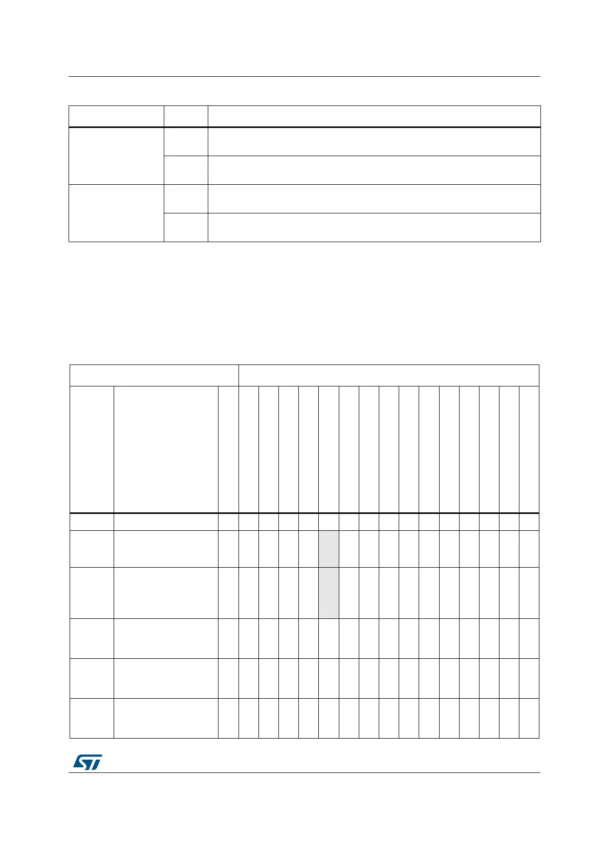
SB19 (BOOT0)
ON
BOOT0 signal of the STM32F411VET6 MCU is held low through a 510
Ω pull-
down resistor
OFF
BOOT0 signal of the STM32F411VET6 MCU is held high through a 10 K
Ω pull-
up resistor
SB20 (BOOT1)
OFF
The BOOT1 signal of the STM32F411VET6 MCU is held high through a 10 K
Ω
pull-up resistor
ON
The BOOT1 signal of the STM32F411VET6 MCU is held low through a 510
Ω
pull-down resistor
1. Default SBx state is shown in bold.
Table 4. Solder bridges (continued)
Bridge State
(1)
Description
Table 5. MCU pin description versus board function (page 1 of 8)
(1)
MCU pin Board function
Main
function
Alternate
functions
LQFP100
CS43L22
MP45DT02
L3GD20
LSM303DLHC
Pushbutton
LED
SWD
USB
OSC
Free I/O
Power supply
CN5
CN2
P1
P2
BOOT0 - 94 - - - - - - - - - - - - - -21
NRST - 14 - - - -
RESET
- - - - - - - - - -
PA0-
WKUP
TIM2_CH1/TIM2_ETR,
TIM5_CH1,
USART2_CTS,
ADC1_0, WKUP
23 - - - -
USER
- - - - - - - - - -
PA1
TIM2_CH2, TIM5_CH2,
USART2_RTS,
ADC1_1
24 - - - - - - - - - - - - - - -
PA2
TIM2_CH3, TIM5_CH3,
TIM9_CH1,
USART2_TX, ADC1_2
25 - - - - - - - - - - - - -14 -
PA3
TIM2_CH4, TIM5_CH4,
TIM9_CH2,
USART2_RX, ADC1_3
26 - - - - - - - - - - - - -13 -