6 Debug management
6.1 Introduction
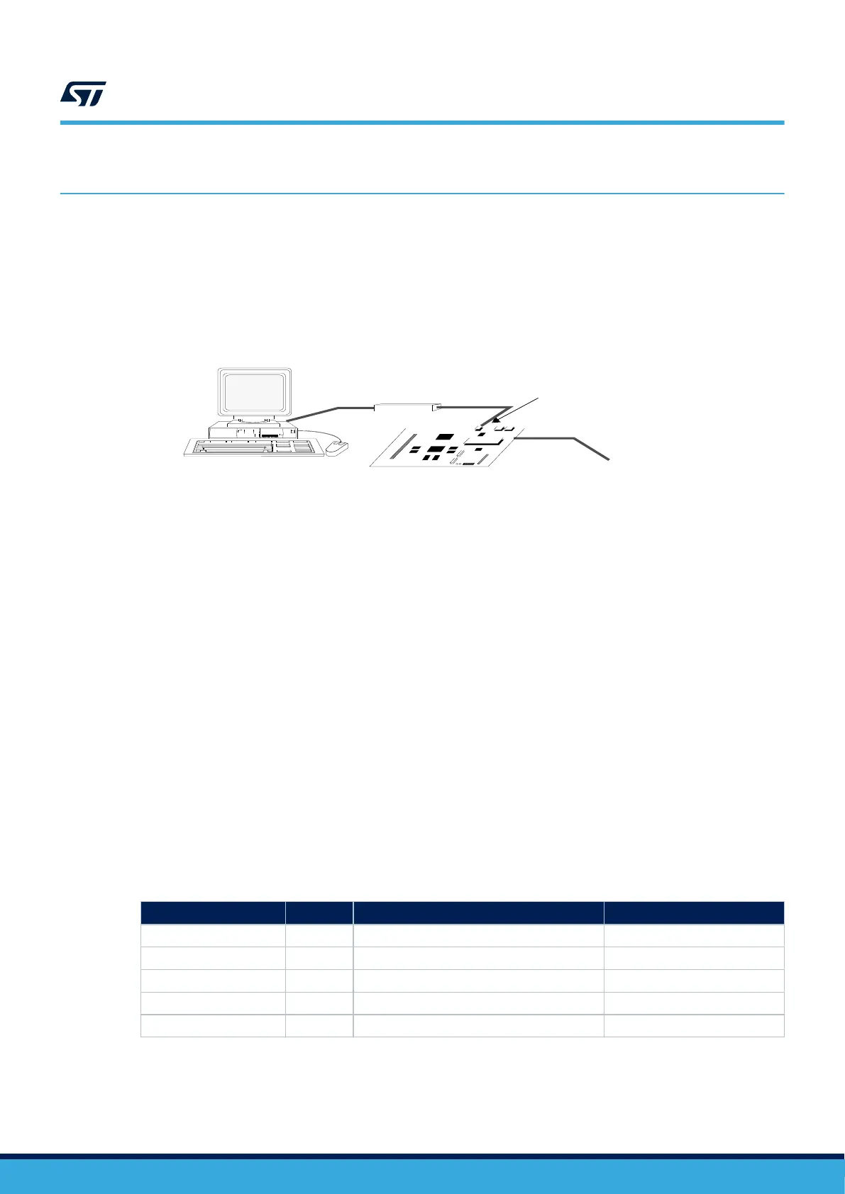
The host / target interface is the hardware equipment that connects the host to the application board. This
interface is made of three components: a hardware debug tool, a JTAG or SW connector and a cable connecting
the host to the debug tool. Figure 14. Host to board connection illustrates the connection of the host to the
evaluation board.
Figure 14. Host to board connection
Evaluation board
Host PC
Power supply
JTAG/SW connector
Debug tool
6.2
SWJ debug port (serial wire and JTAG)
The core of the STM32H723/33, STM32H725/35 and STM32H730 microcontrollers integrates the serial wire /
JTAG debug port (SWJ-DP). It is an Arm
®
standard CoreSight
™
debug port that combines a 5-pin JTAG-DP
interface and a 2-pin SW-DP interface.
• The JTAG debug port (JTAG-DP) provides a 5-pin standard JTAG interface to the AHP-AP port.
• The serial wire debug port (SW-DP) provides a 2-pin (clock + data) interface to the AHP-AP port.
In the SWJ-DP, the two SW-DP JTAG pins the are multiplexed with some of the JTAG-DP five JTAG pins.
For more details on the SWJ debug port refer to the reference manual STM32H723/733, STM32H725/735 and
STM32H730 advanced Arm
®
-based 32-bit MCUs (RM0468) SWJ debug port section (serial wire and JTAG).
6.2.1 TPIU trace port
The TPIU trace port comprises four data outputs plus one clock output. The number of data outputs can be
configured by software and unused signals can be reused as GPIOs. If the trace port is not required, all the
signals can be used as GPIOs. By default, the trace port is disabled.
The trace data and clock can operate at up to 133 MHz. As a result, care must be taken with the layout of these
signals: the trace connector should be located as close as possible to the microcontroller, while still allowing
enough space to attach the trace port analyzer probe.
Refer to Table 7. TPIU trace pins for a summary of trace pins and GPIO assignment.
Table 7. TPIU trace pins
Trace pin name Type Description Pin assignment
TRACED0 Output Trace synchronous data out 0 PC1 or PE3 or PG13
TRACED1 Output Trace synchronous data out 1 PC8 or PE4 or PG14
TRACED2 Output Trace synchronous data out 2 PD2 or PE5
TRACED3 Output Trace synchronous data out 3 PC12 or PE6
TRACECLK Output Trace clock PE2
6.2.2 External debug trigger
The bidirectional TRGIO signal can be configured as TRGIN or TRGOUT by software. Refer to Table 8. External
debug trigger pins for a summary of trigger pins and GPIO assignment.
AN5419
Debug management
AN5419 - Rev 2
page 28/50
 Loading...


