2.1.1 External power supplies and components
Refer to the STM32H72x and STM32H73x datasheets for more details on the electrical characteristics.
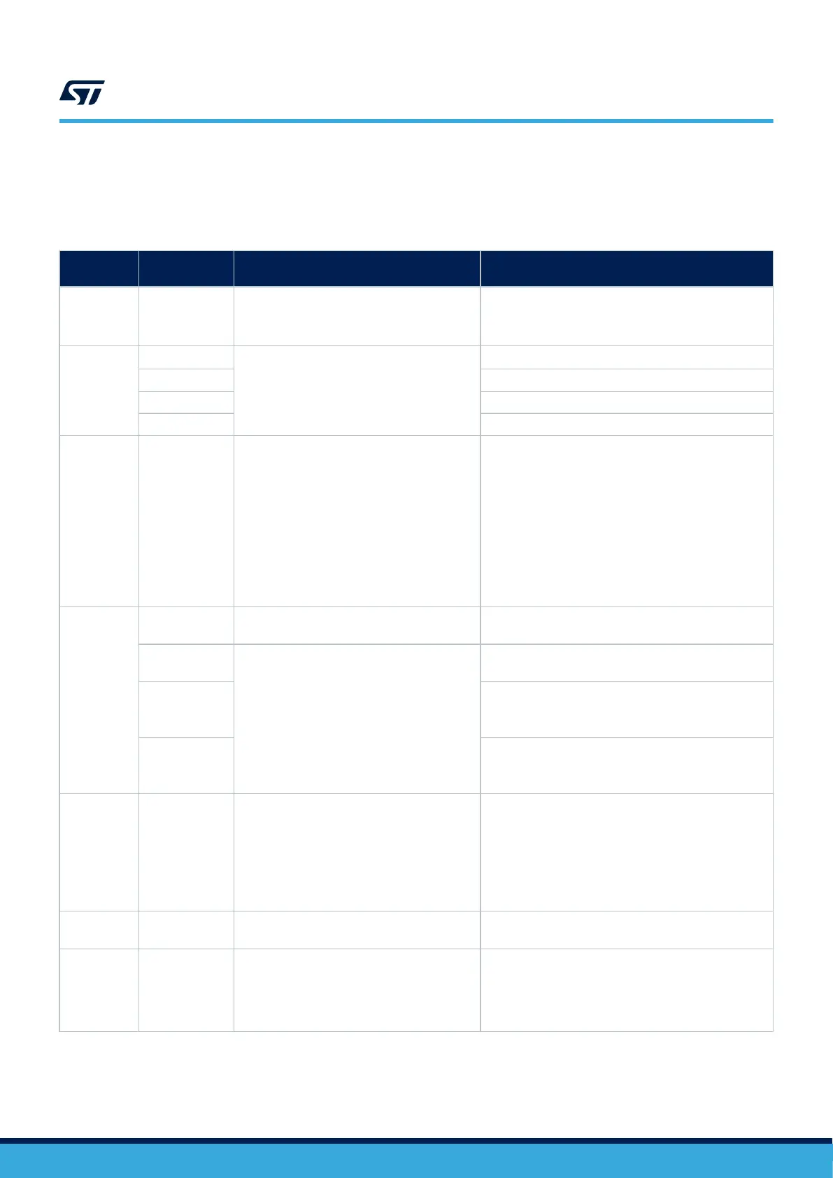
Table 2. Power supply connection
Package pin/
ball
Voltage range External components Comments
VDD 1.62 to 3.6 V
100 nF ceramic, for each V
DD
as
close as possible of the pins. A 4.7 μF ceramic
connected to one of the VDD pin.
For V
DD
< 1.71 V the PDR must be disabled (see Section
2.2.1 Power-on reset (POR)/power-down reset (PDR))
VDDA
1.62 to 3.6 V
1 μF ceramic and 100 nF as close as possible
of the pin
V
DDA
can be connected to V
DD
through a ferrite bead.
1.8 to 3.6 V Restriction if a DAC or VREFBUF is used.
2.0 to 3.6 V Restriction if an OPAMP used.
0 to 3.6 V DAC, ADC, OPAMP, COMP, VREFBUF are not used.
VBAT 1.2 to 3.6 V 1 μF ceramic and 100 nF close to the VBAT pin
Can be connected directly to an external battery or
supply.
The external battery can be charged through the internal
5 kΩ or 1.5 kΩ resistor (see the reference manual
STM32H723/733, STM32H725/735 and STM32H730
advanced Arm
®
-based 32-bit MCUs (RM0468).
To be connected to V
DD
when not used.
When the PDR_ON pin is set to V
SS
the VBAT pin must
be connected to V
DD
since this functionality is no longer
available.
VDDSMPS
0 V No capacitor required.
VDDSMPS connected to V
SS
when the converter is not
used.
1.62 to 3.6 V =
V
DD
Four different solutions are recommended:
• 10 μF (best cost trade-off), ESR 10mΩ
• 2x 10 μF (best area/performance trade-
off)
• 10 μF + 100 nF close from pin (best cost/
performance trade-off)
• 10 μF + 4.7 μF (best performance)
For SMPS supplying V
CORE
.
2.3 to 3.6 V =
V
DD
For SMPS output regulated to 1.8 V.
The SMPS supplies the LDO regulator or an external
regulator.
3 to 3.6 V = V
DD
For SMPS output regulated to 2.5 V.
The SMPS supplies the LDO regulator or an external
regulator.
VLXSMPS
V
CORE
or 1.8 V
or 2.5 V
When the SMPS is used:
• 2.2 μH (DCR 110mΩ, I
sat
1.7 A, I
temp
1.4 A) as close as possible to V
LXSMPS
.
• LQFP/BGA packages: 220 pF ceramic
capacitor on VLXSMPS.
• 2x 10 μF (ESR 5 mΩ) close to the
inductor on VFBSMPS connection side.
Depending on the use case, the SMPS provides the
digital core supply or a supply provided to another
regulator (external or internal LDO).
See Figure 2. System supply configuration for connection
VFBSMPS
V
CORE
or 1.8 V
or 2.5 V
-
Refer to Figure 2. System supply configuration for the
use case dependent of this pin.
VDDLDO 1.62 to 3.6 V
When the LDO is used: 1x 4.7 μF capacitor
close to one VDDLDOx pin, all VDDLDOx pins
correctly connected together.
Otherwise: no capacitor is required. Connect
VDDLDOx to VDD.
V
DDLDO
≤ V
DD
.
Up to three VDDLDO pins available depending on the
package specification.
AN5419
Introduction
AN5419 - Rev 2
page 7/50
 Loading...


