DocID030511 Rev 1 23/69
UM2198 Hardware layout and configuration
68
A 128-Mbit NOR Flash is connected to the NOR/PSRAM1 bank1 of the FMC interface. The
16-bit operation mode is selected by pull-up resistor connected to the BYTE pin of NOR
Flash. The write protection can be enabled or disabled, depending on how the jumper JP13
is set, as showed in Table 13.
All signals for memory are also connected on memory connectors CN11 and CN12 for
memory daughterboards.
Limitations can happen when using other peripherals:
1. FMC addressing limitation depending on number of trace data bus used (A18 max for 4
bit ETM to A21 max for 1 bit ETM)
2. FMC addresses limited to A18 when SAI used
3. FMC addresses limited to A22 when PDM is used
In such cases, serial resistors R236 (A19), R231 (A20), R217 (A21) and R230 (A22) should
be removed. Thus memory addresses A19 to A22 are not connected to FMC and they are
pulled down on the board. Memories can be addressed within a limited address range.
By default, all these serial resistors are soldered on the board. If A19 is required, it is
necessary to configure (SAI_SDB) ADCDAT1 pin of audio codec WM8994ECS/R (U22) by
software to be tri-state.
8.17 Twin Quad-SPI NOR Flash
The Quad-SPI Flash is implemented on the STM32H743XI microcontroller of the Evaluation
board either as 1 Twin Quad-SPI NOR Flash (1-Gbit (2*512Mb)) memory or as 2 Quad-SPI
NOR Flash (512Mb) memories.
The two dies in the Twin Quad-SPI Flash memory share the same clock and chip select
signals of the STM32H743XI microcontroller.
8.18 Analog input
The two-pin header CN5 and 10 K ohm potentiometer RV1 is connected to PA0_C of
STM32H743XI as analog input. A low-pass filter can be implemented by replacing R11 and
C7 with the right value of resistor and capacitor as requested by the end-user application.
8.19 Display and input devices
Four general-purpose-color LEDs (LD 1, 2, 3 and 4) are available as display device. LD1
and LD3 are connected on STM32H743XI, LD2 and LD4 are connected on MFX.
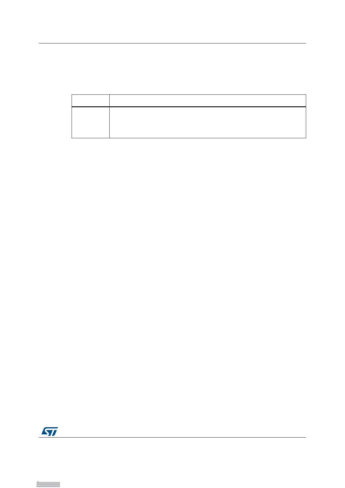
Table 13. NOR Flash related jumpers
Jumper Description
JP13
Write protection is enabled when JP13 is fitted while write protection is disabled
when JP13 is not fitted.
Default Setting: Not fitted
Downloaded from Arrow.com.Downloaded from Arrow.com.Downloaded from Arrow.com.Downloaded from Arrow.com.Downloaded from Arrow.com.Downloaded from Arrow.com.Downloaded from Arrow.com.Downloaded from Arrow.com.Downloaded from Arrow.com.Downloaded from Arrow.com.Downloaded from Arrow.com.Downloaded from Arrow.com.Downloaded from Arrow.com.Downloaded from Arrow.com.Downloaded from Arrow.com.Downloaded from Arrow.com.Downloaded from Arrow.com.Downloaded from Arrow.com.Downloaded from Arrow.com.Downloaded from Arrow.com.Downloaded from Arrow.com.Downloaded from Arrow.com.Downloaded from Arrow.com.

 Loading...


