Debug management AN4938
30/46 AN4938 Rev 4
6.3.2 Flexible SWJ-DP pin assignment
After RESET (SYSRESETn or PORESETn), all the five pins used for the SWJ-DP are
assigned as dedicated pins immediately usable by the debugger host (note that the trace
outputs are not assigned except if explicitly programmed by the debugger host).
However, the STM32H74xI/G and STM32H75xI/G devic
es offer the possibility of disabling
some or all of the SWJ-DP ports and so, of releasing the associated pins for general-
purpose IO (GPIO) usage.
Table 7 s
hows the different possibilities to release some pins.
For more details on how to disable SWJ-DP port pins, please refer to the reference manual
I/O pin alternate function multiplexer and mapping section.
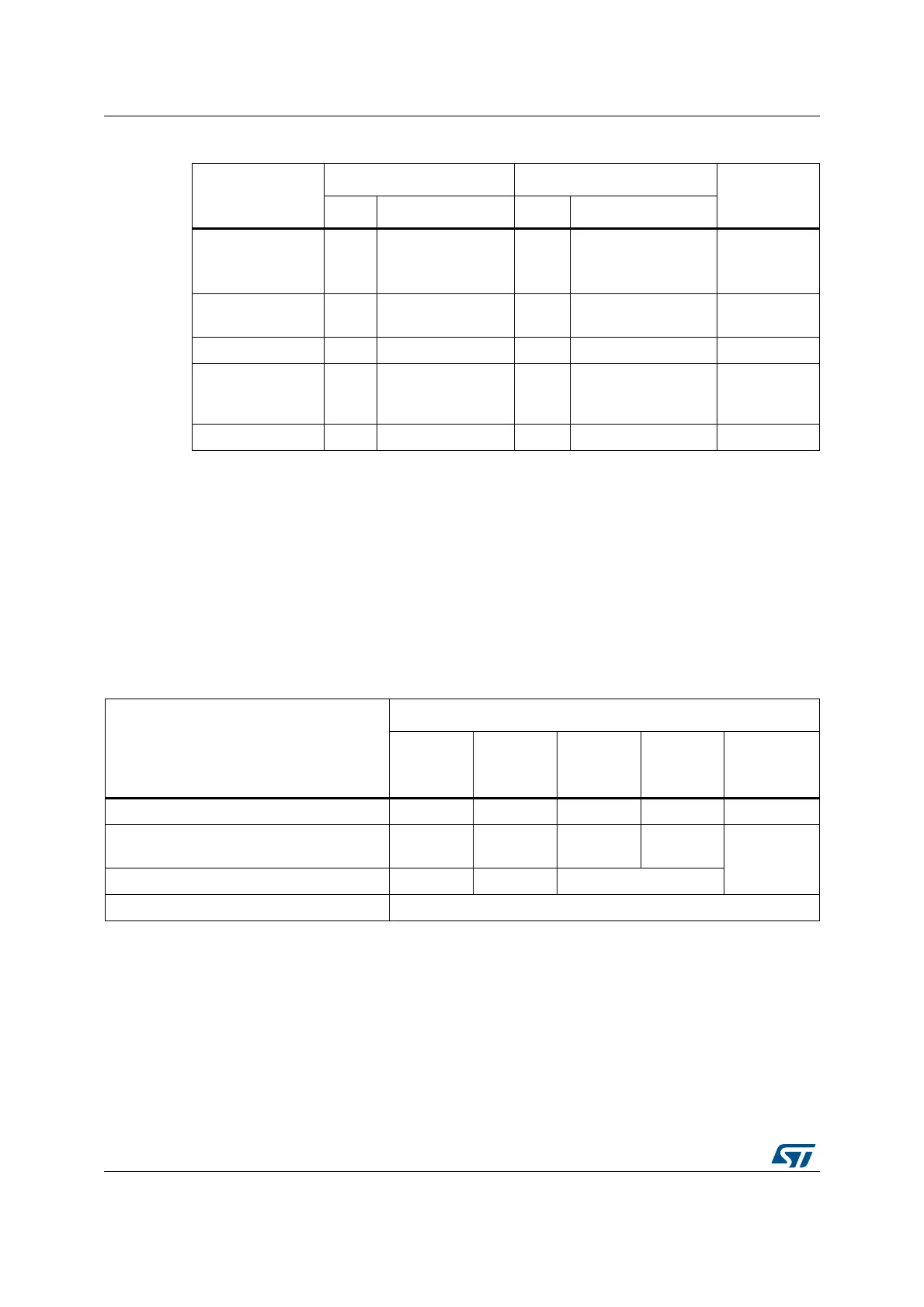
Table 6. SWJ debug port pins
SWJ-DP pin name
JTAG debug port SW debug port
Pin
assignment
Type Description Type Debug assignment
JTMS/SWDIO I
JTAG test mode
Selection
IO
Serial wire data
input/output
PA13
JTCK/SWCLK I JTAG test clock I Serial wire clock PA14
JTDI I JTAG test data input - - PA15
JTDO/TRACESWO O
JTAG test data
output
-
TRACESWO if
asynchronous trace is
enabled
PB3
NJTRST I JTAG test nReset - - PB4
Table 7. Flexible SWJ-DP assignment
Available debug ports
SWJ IO pin assigned
PA13/
JTMS/
SWDIO
PA14/JTCK
/SWCLK
PA15/JTDI PB3/JTDO PB4/NJTRST
Full SWJ (JTAG-DP + SW-DP) - reset state X X X X X
Full SWJ (JTAG-DP + SW-DP) but without
NJTRST
XXXX
-
JTAG-DP disabled and SW-DP enabled X X -
JTAG-DP disabled and SW-DP disabled Released
 Loading...


