Debug system overview UM0470
6/39 DocID14024 Rev 4
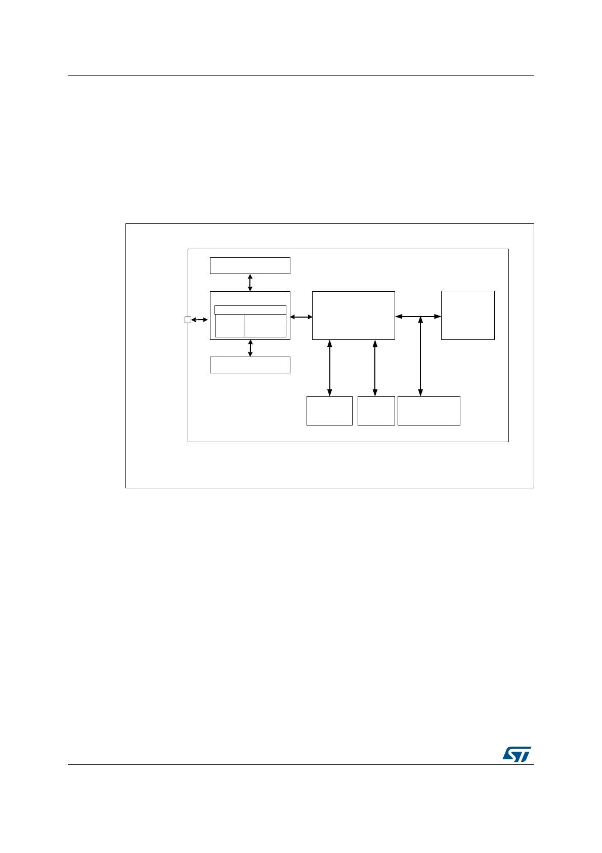
1 Debug system overview
The STM8 MCUs debug system interface allows a debugging or programming tool to be
connected to the MCU through a single wire. This connection results in a bidirectional
communication based on an open-drain line and provides a non-intrusive read/write access
to RAM and peripherals during the program execution.
The block diagram is shown in Figure 1.
Figure 1. Debug system block diagram
The debug module uses the two internal clock sources present in the device:
• the low speed internal clock (LSI clock): usually in the range of 30 kHz to 200 kHz
depending on the product
• the high speed internal clock (HSI clock): usually in the range of 10 MHz to 25 MHz
depending on the device.
The clocks are automatically started when necessary.
06Y9
'HEXJPRGXOH
'0
&38EXV
3HULSKHUDOEXV
5DPEXV
60,0SLQ
/6,RVFLOODWRU
+6,RVFLOODWRU
3HULSKHUDOV
5$0
)ODVK
'DWD((3520
670
FRUH
6700&8
6:,0
6:,0HQWU\
&RPP
OD\HU
&RPPDQG
GHFRGH