24
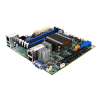
A2SDV-8C/-12C+/-16C-TLN5F User's Manual
BAR CODE
COM2
DESIGNED IN USA
A2SDV-8C-TLN5F
REV:1.02
JIPMB1
JMD2
JMD1
JTGLED1
JPW1
JPI2C1
JSD1
SRW2
SRW3
SRW4
SRW1
JUIDB
JPL1
1
JWD1
JPG1
JBR1
JPME2
JI2C1
JI2C2
DIMMB1
DIMMB2
DIMMA1
DIMMA2
LED1
1
JD1
JSMB1
JBT1
JPH1
JPV1
FANB
JTPM1
JNCSI1
JL1
JRT4
1
JRT3
I-SATA1 I-SATA0
UIDLED1
CM CODE
LEDBMC
eUSB
ON
PWR
JF1
RST X
OH/FF
2
NIC NIC
1 LED
HDD
LED
X
PWR
NMI
ALWAYS POPULATE DIMMx1 FIRST
CPU SLOT6 PCI-E 3.0 X8
CPU SLOT7 PCI-E 3.0 X8
VGA
KEY-M PCIE3/SATA3
KEY-B SATA3/USB3
COM1
LAN1(IPMI_LAN)
LAN5
CPU
USB6(3.0)
USB2/3(3.0)
USB0/1(3.0)
USB 4/5
LAN3
FAN4 FAN3
FAN2 FAN1
LAN4/
LAN2/
FANA
SATA DOM POWER
BT1
JF1
BMC AST2400
JPTG1
JSEL1
DIMMB1
DIMMA1
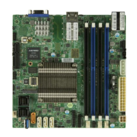
DIMM Module Population Sequence
When installing memory modules, the DIMM slots should be populated in the following order:
DIMMA1, DIMMB1, DIMMA2, DIMMB2.
• Always use DDR4 DIMM modules of the same type, size and speed.
• Mixed DIMM speeds can be installed. However, all DIMMs will run at the speed of the
slowest DIMM.
• The motherboard will support odd-numbered modules (one or three modules installed).
However, for best memory performance, install DIMM modules in pairs to activate memory
interleaving.
DIMMA2
DIMMB2
 Loading...