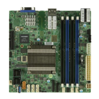
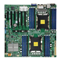
39
Chapter 2: Installation
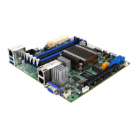
BAR CODE
COM2
DESIGNED IN USA
A2SDV-8C-TLN5F
REV:1.02
JIPMB1
JMD2
JMD1
JTGLED1
JPW1
JPI2C1
JSD1
SRW2
SRW3
SRW4
SRW1
JUIDB
JPL1
1
JWD1
JPG1
JBR1
JPME2
JI2C1
JI2C2
DIMMB1
DIMMB2
DIMMA1
DIMMA2
LED1
1
JD1
JSMB1
JGP1
JBT1
JPH1
JPV1
FANB
JTPM1
JNCSI1
JL1
JRT4
1
JRT3
I-SATA1 I-SATA0
UIDLED1
CM CODE
LEDBMC
eUSB
ON
PWR
JF1
RST X
OH/FF
2
NIC NIC
1 LED
HDD
LED
X
PWR
NMI
ALWAYS POPULATE DIMMx1 FIRST
CPU SLOT6 PCI-E 3.0 X8
CPU SLOT7 PCI-E 3.0 X8
VGA
KEY-M PCIE3/SATA3
KEY-B SATA3/USB3
COM1
LAN1(IPMI_LAN)
LAN5
CPU
USB6(3.0)
USB2/3(3.0)
USB0/1(3.0)
USB 4/5
LAN3
FAN4 FAN3
FAN2 FAN1
LAN4/
LAN2/
FANA
SATA DOM POWER
BT1
JF1
BMC AST2400
JPTG1
JSEL1
Chassis Intrusion
A Chassis Intrusion header is located at JL1 on the motherboard. Attach the appropriate cable
from the chassis to inform you of a chassis intrusion when the chassis is opened. Refer to
the table below for pin denitions.
Chassis Intrusion
Pin Denitions
Pin# Denition
1 Intrusion Input
2 Ground
1
1. Chassis Intrusion
2. General Purpose I/O
General Purpose I/O Header
JGP1 is a 10-pin general purpose I/O header. Each pin can be congured to be an input or
output pin. The GPIO is controlled via the PCA9554 8-bit GPIO expansion. The base address
is 0xF040(D31:F4).
2
JGP1 Header
Pin Denitions
Pin# Denition
1 +5V +5V
2 Ground Ground
3 GP0 GPP_E0
4 GP1 GPP_F1
5 GP2 GPP_E1
6 GP3 GPP_F2
7 GP4 GPP_E2
8 GP5 GPP_F3
9 GP6 GPP_F0
10 GP7 GPP_F4
 Loading...