17
Chapter 1: Introduction
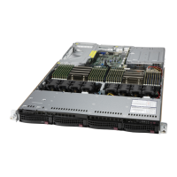
Figure 1-7. Motherboard Layout
1.4 Motherboard Layout
Below is a layout of the H13SSH motherboard with a jumper, connector, and LED locations
shown. See the table on the following page for descriptions. For detailed descriptions, pinout
information, and jumper settings, refer to Chapter 4 or the Motherboard Manual.
BAR CODE BAR CODE
BIOS LICENSE
BAR CODE BAR CODE
H13SSH
REV:1.01
DESIGNED IN USA
+
A
C
JAIOM1
PSU1
JIO1
JSXB0
JPWR1
BT1
J7
FAN7
JUSB2
FAN6
FAN5
JPWR6
JPWR5
FAN4
FAN3
JNVI2C1
FAN2
FAN1
CPU
PSU2
JNCSI1
JTPM1
JAIOM2SB1
JSXB1
JPWR2
JPWR3
NVMe0/1
JNVVPP1
LED4
LED1
JRSI2C1
JPWR7
JPWR10
JPWR11
FAN9
JPWR4
JPWR9
DIMML2
DIMMK1
DIMMK2
DIMML1
DIMMI2
DIMMJ2
DIMMJ1
DIMMI1
DIMMH2
DIMMH1
DIMMG2
DIMMG1
NVMe 18/19
NVMe 16/17
NVMe 14/15
NVMe 12/13
JPWR8
DIMMF2
DIMMF1
DIMME2
DIMME1
DIMMD2
DIMMA1
DIMMA2
DIMMB1
DIMMB2
DIMMC1
DIMMD1
DIMMC2
JFP1
JFP2
FAN8
NVMe10/11
NVMe6/7
NVMe4/5
NVMe8/9
NVMe2/3
JPG1
JUID1

 Loading...