47
Chapter 2: Installation
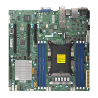
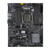
Standby Power Header
The +5V Standby Power header is located at JSTBY1 on the motherboard. You must have
a card with a Standby Power connector and a cable to use this feature. Refer to the table
below for pin denitions.
Standby Power Header
Pin Denitions
Pin# Denition
1 +5V Standby
2 Ground
3 NC
Disk-On-Module Power Connector
One power connector for a SATA DOM (Disk-On-Module) device is located at JSD1. Connect
the appropriate cable here to provide power support for your Serial Link DOM device.
DOM Power Connector
Pin Denitions
Pin# Denition
1 5V
2 Ground
3 Ground
JSTBY1
LE2
A
C
LE1
C
LEDPWR
LEDBMC
A C
JL1
JBT1
JSD1
JIPMB1
JRK1
JWD1
JPAC1
1
JVRM1
JPG1
1
JPME2
I-SATA3
I-SATA2
I-SATA1
JNVME1
PRESS FIT
JTPM1
AUDIO_FP1
I-SGPIO1
I-SGPIO2
SP1
+
BT1
+
JF1
JD1
FAN1
FAN2
FAN3
FAN4
FANA
JPWR1
JPWR2
JPI2C1
JTBT
MH13
MH10
MH11
MH12
X11SRA
REV:1.01
BIOS LICENSE
BAR CODE
IPMI CODE
MAC CODE
DESIGNED IN USA
USB 4/5
USB 2/3
USB 0/1
COM1
I-SATA6~7
I-SATA4~5
I-SATA2~3
CPU M.2 PCI-E 3.0 x4
CPU M.2 PCI-E 3.0 x4
HD AUDIO
VGA
LAN1
LAN2
USB 10/11(3.0)
USB 12/13(3.1)
USB 8/9(3.0)
USB 6/7(3.0)
CPU SLOT6 PCI-E 3.0 x16
CPU SLOT4 PCI-E 3.0 x16
CPU SLOT2 PCI-E 3.0 x8 (IN x16)
PCH SLOT1 PCI-E 3.0 x4
DIMMD2
DIMMD1
DIMMC2
DIMMC1
DIMMB2
DIMMB1
DIMMA2
DIMMA1
CLOSE 1st
OPEN 1st
PCH
C422
JNVI2C1
KB/MOUSE
A
CPU
LGA 2066
BMC
J13
J12
1
2
1. Standby Power Header
2. JSD1
 Loading...