62 Network Circuitry TB9100 Reciter Service Manual
© Tait Electronics Limited January 2006
5.3.2 Synchronous DRAM (SDRAM)
The main memory for executable code and data is normally provided by two
256Mbit SDRAM chips (U300 and U302), each 4M x 16 bits x 4 banks.
Together, these provide 64Mbytes (16Meg of 32-bit words) of memory.
The SDRAM PCB footprints also provide for expansion to 512Mbit parts,
each 8M x 16bits x 4 banks, giving a total of 128Mbytes of memory; or a
decrease to 64Mbit parts, each 1M x 16bits x 4 banks, giving 16Mbytes total.
Configuration changes for different size SDRAM chips is mainly
accommodated through reprogramming the UPM (see “User-
Programmable Machines” on page 51). The exception is for the 64Mbit
parts, which require a hardware change as shown in Table 5.10 .
Reference should be made to the data sheet (reference 4) for details of the
SDRAM chips. A full description of the operation of SDRAMs is outside
the scope of this document; the application notes (references 5 and 6) should
be referred to for a more detailed explanation.
SDRAM Control
Inputs
The x16 SDRAM chips are paired to provide a 32-bit data bus to match the
MPC’s data bus width. The MPC always reads and writes 32-bit words, but
individual bytes can be written by using the byte select lines, BS[0..3]
. These
byte selects are connected to the appropriate byte mask inputs (DQML and
DQMU) of the SDRAMs; when these inputs are high they prevent data
being written into the corresponding byte of the memory location.
Other control lines, row address strobe (RAS
), column address strobe
(CAS
), write enable (WE) and chip select (CS), control the mode of
operation of the SDRAM. All the control signals are synchronously timed
using the clock input (CLK): signals are latched on the rising edge of CLK.
An exception is the clock enable signal, CKE; if this is taken low the
SDRAM goes into a low-power standby mode and ignores all other inputs,
including the CLK signal. This mode is not used in the ASIF and hence
CKE is permanently tied high.
The CLK signal is generated by the MPC. For EMC reduction the clock
line is series terminated by resistor R204. An AC-coupled shunt
termination, R303 and C317, cleans up residual reflections on the clock
line.
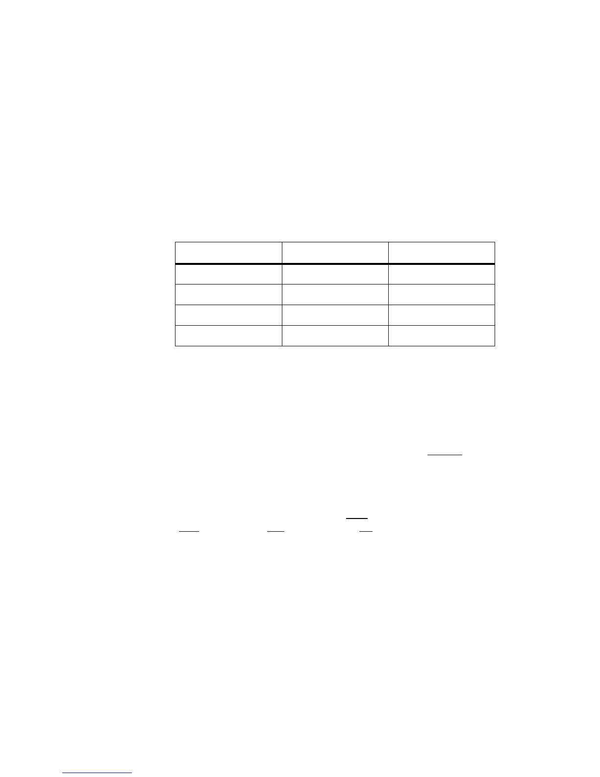
Table 5.10 SDRAM Hardware Configuration
SDRAM Size (Mbits) R301 R302
64 not fitted 33R
128 33R not fitted
256 33R not fitted
512 33R not fitted
 Loading...


