Theory of Operation—2465B/2467B Service
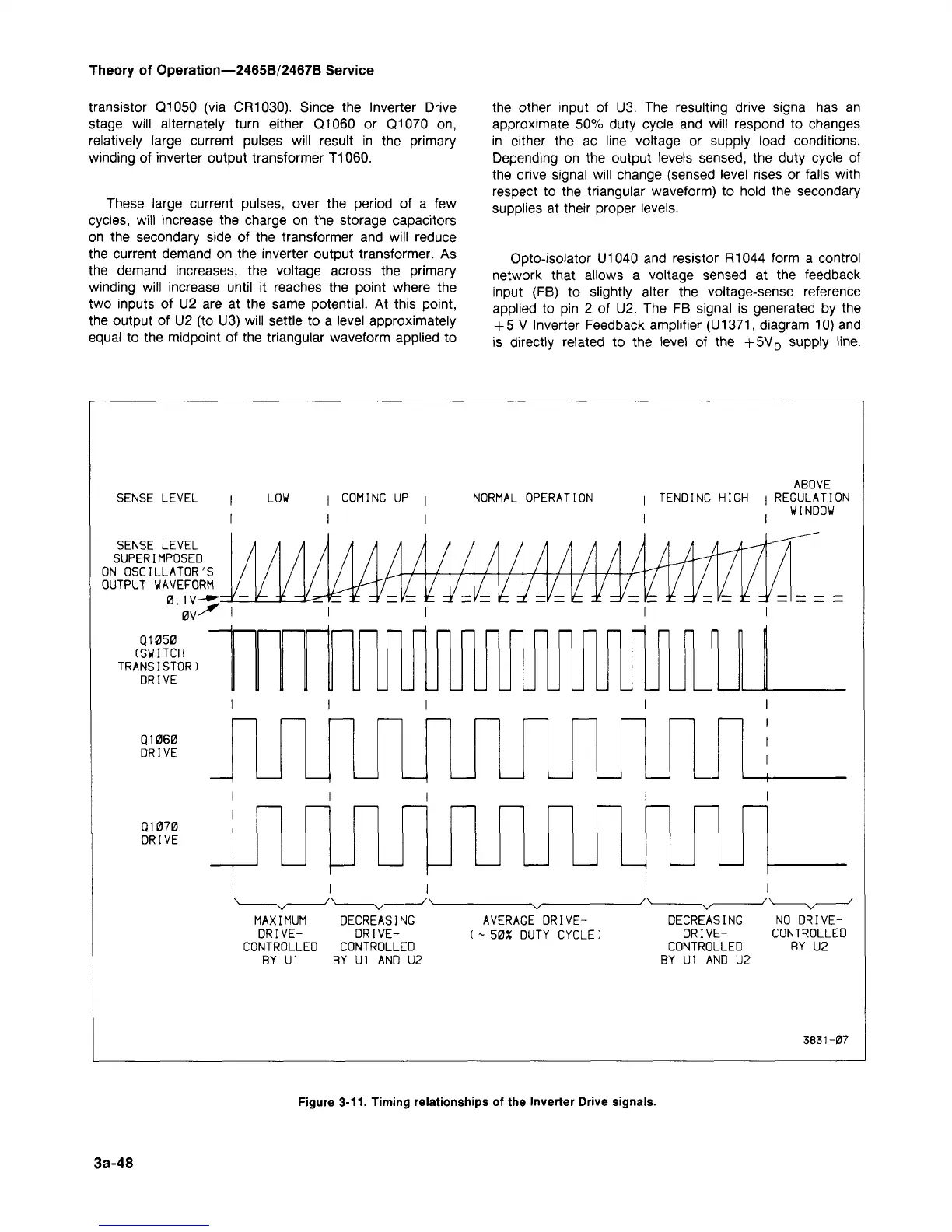
transistor Q1050 (via CR1030). Since the Inverter Drive
stage will alternately turn either Q1060 or Q1070 on,
relatively large current pulses will result in the primary
winding of inverter output transformer T1060.
These large current pulses, over the period of a few
cycles, will increase the charge on the storage capacitors
on the secondary side of the transformer and will reduce
the current demand on the inverter output transformer. As
the demand increases, the voltage across the primary
winding will increase until it reaches the point where the
two inputs of U2 are at the same potential. At this point,
the output of U2 (to U3) will settle to a level approximately
equal to the midpoint of the triangular waveform applied to
the other input of U3. The resulting drive signal has an
approximate 50% duty cycle and will respond to changes
in either the ac line voltage or supply load conditions.
Depending on the output levels sensed, the duty cycle of
the drive signal will change (sensed level rises or falls with
respect to the triangular waveform) to hold the secondary
supplies at their proper levels.
Opto-isolator U1040 and resistor R1044 form a control
network that allows a voltage sensed at the feedback
input (FB) to slightly alter the voltage-sense reference
applied to pin 2 of U2. The FB signal is generated by the
+
5
V Inverter Feedback amplifier
(U1371,
diagram 10) and
is directly related to the level of the +5V
D
supply line.
SENSE LEVEL
SENSE LEVEL
SUPERIMPOSED
ON
OSCILLATOR'S
OUTPUT WAVEFORM
0.1V-J
0V^
LOW
COMING
UP 1
NORMAL OPERATION TENDING HIGH
ABOVE
REGULATION
WINDOW
Q1050
(SWITCH
TRANSISTOR)
DRIVE
01060
DRIVE
Q1070
DRIVE
v
MAXIMUM
DRIVE-
CONTROLLED
BY
U1
v
DECREASING
DRIVE-
CONTROLLED
BY
U1 AND U2
I
AVERAGE
DRIVE-
(
- 50X
DUTY CYCLE
)
v
DECREASING
DRIVE-
CONTROLLED
BY
U1 AND U2
v
NO DRIVE-
CONTROLLED
BY U2
3831-07
Figure 3-11. Timing relationships of the Inverter Drive signals.
3a-48