LE910Cx Hardware Design Guide
1VV0301298 Rev.40 Page 58 of 149 2023-03-16
Not Subject to NDA
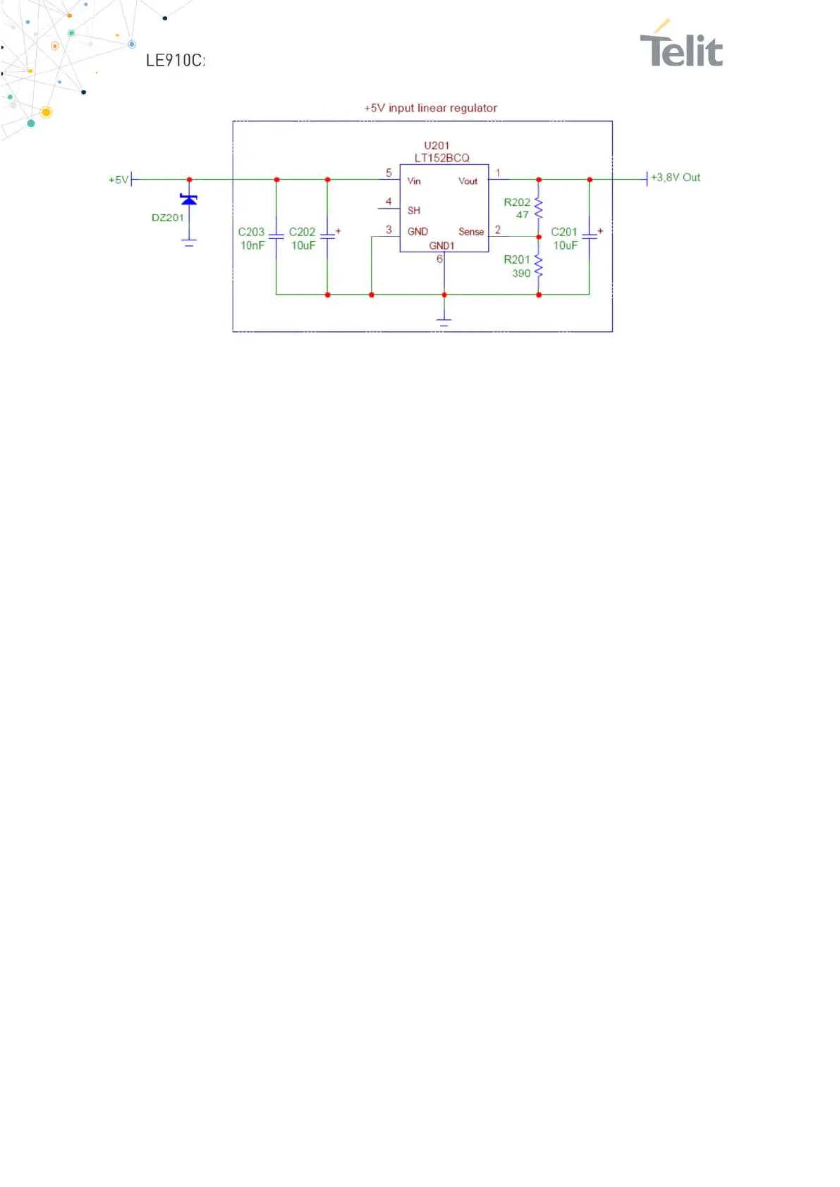
Figure 14: Example of Linear Regulator with 5V Input
6.3.1.2. + 12V Input Source Power Supply – Design Guidelines
The desired output for the power supply is 3.8V. Due to the huge difference
between the input source and the desired output, a linear regulator is unsuitable
and must not be used. A switching power supply is preferable for its better
efficiency, especially with the 2A peak current load expected during GSM Tx.
When using a switching regulator, a 500-kHz or higher switching frequency
regulator is preferable because of its smaller inductor size and its faster transient
response. This allows the regulator to respond quickly to the peak current
consumption.
In any case, the selection of the frequency and switching design is related to the
application to be developed as the switching frequency can also generate EMC
interference.
For car batteries (lead-acid accumulators) the input voltage can rise up to 15.8V.
This must be kept in mind when choosing components: all components in the
power supply must withstand this voltage.
A bypass low ESR capacitor of adequate capacity must be provided to cut the
current absorption peaks. A 100μF capacitor is usually suitable on VBATT &
VBATT_PA power lines.
Make sure that the low ESR capacitor on the power supply output is rated at least
10V.
For automotive applications, a spike protection diode must be inserted close to the
power input to clean the supply of spikes.
 Loading...