LE910Cx Hardware Design Guide
1VV0301298 Rev.40 Page 86 of 149 2023-03-16
Not Subject to NDA
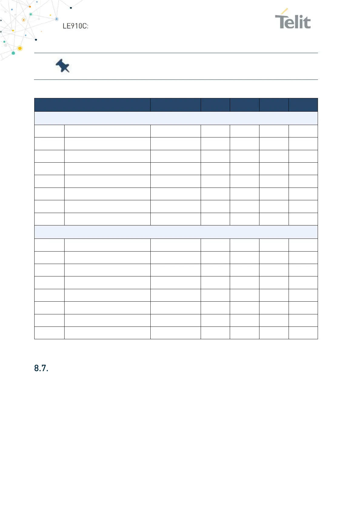
Figure 22: I2S timing diagram
Note LE910Cx family supports both PCM/I2S.
Parameter Comments Min Typ Max Unit
Using internal SCK
Frequency - - 12.288 MHz
T Clock period 81.380 - - ns
t(HC) Clock high 0.45*T - 0.55*T ns
t(LC) Clock low 0.45*T - 0.55*T ns
t(sr) SD and WS input setup time 16.276 - - ns
t(hr) SD and WS input hold time 0 - - ns
t(dtr) SD and WS output delay - 65.100 ns
t(htr) SD and WS output hold time 0 - - ns
Using external SCK
Frequency - - 12.288 MHz
T Clock period 81.380 - - ns
t(HC) Clock high 0.45*T - 0.55*T ns
t(LC) Clock low 0.45*T - 0.55*T ns
t(sr) SD and WS input setup time 16.276 - - ns
t(hr) SD and WS input hold time 0 - - ns
t(dtr) SD and WS output delay - 65.100 ns
t(htr) SD and WS output hold time 0 - - ns
Table 36: Interface timing
General Purpose I/O
The general-purpose I/O pads can be configured to act in three different ways:
Input
Output
Alternative function (internally controlled)
 Loading...