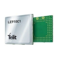
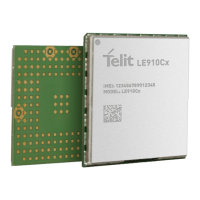
LE910Cx Hardware Design Guide
1VV0301298 Rev.40 Page 104 of 149 2023-03-16
Not Subject to NDA
Stencil
The layout of the stencil openings can be the same as the recommended footprint (1:1).
The suggested thickness of stencil foil is greater than 120 µm.
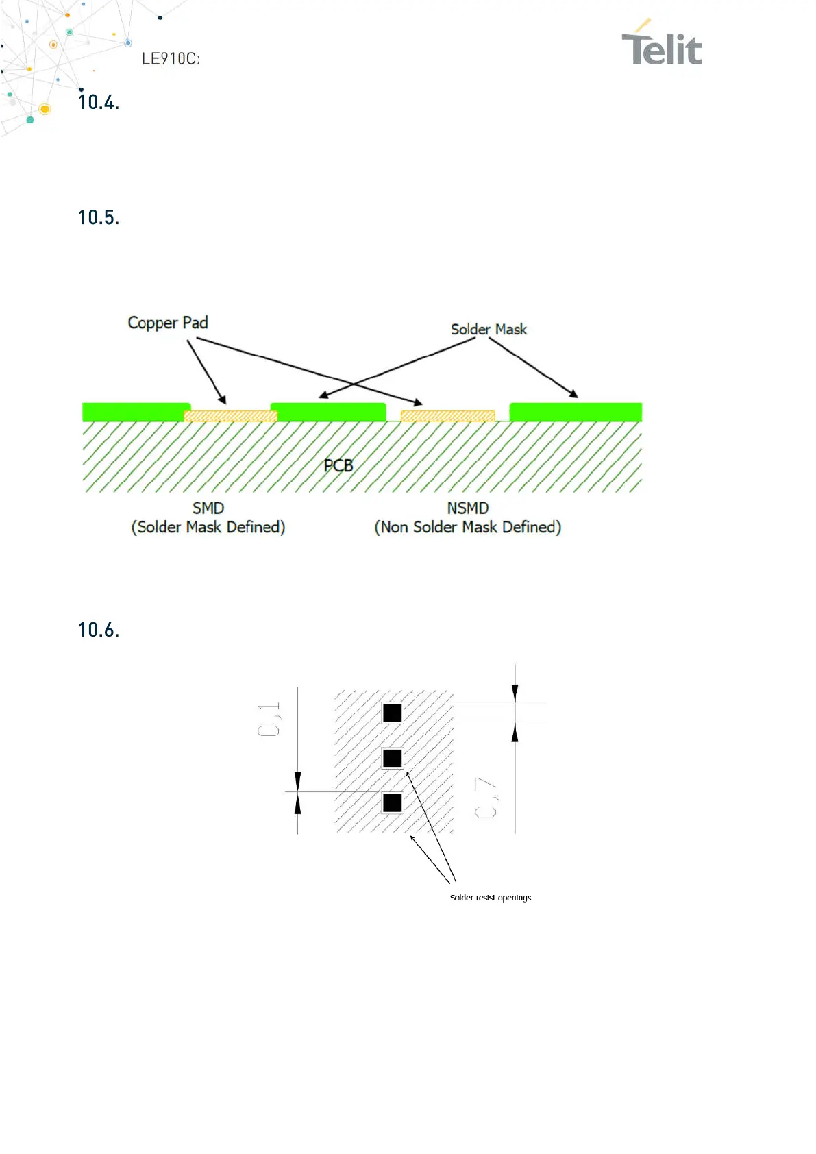
PCB Pad Design
The solder pads on the PCB are recommended to be of the Non-Solder Mask Defined
(NSMD) type.
Figure 34: PCB Pad Design
Recommendations for PCB Pad Dimensions (mm)
Figure 35: PCB Pad Dimensions
 Loading...