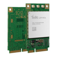
LE910Cx Hardware Design Guide
1VV0301298 Rev.37 Page 7 of 149 2023-03-16
Not Subject to NDA
Indication of Software Ready 91
RTC – Real Time Clock 91
VAUX Power Output 91
ADC Converter 91
9.5.1.
Description 91
9.5.2.
Using the ADC Converter 92
Using the Temperature Monitor Function 92
GNSS Characteristics 92
10.
MOUNTING THE MODULE ON YOUR BOARD 94
General 94
Finishing & Dimensions 94
Recommended Footprint for the Application 100
Stencil 104
PCB Pad Design 104
Recommendations for PCB Pad Dimensions (mm) 104
Solder Paste 105
10.7.1.
Solder Reflow 105
10.7.2.
Cleaning 106
11.
APPLICATION GUIDE 108
Debug of the LE910Cx Module in Production 108
Bypass Capacitor on Power Supplies 108
SIM Interface 109
11.3.1.
SIM Schematic Example 109
EMC Recommendations 110
Download and Debug Port 110
11.5.1.
Recovery Boot Mode 111
12.
PACKING SYSTEM 112
Packing System – Tray 112
Tape & Reel 115
Moisture Sensitivity 120
13.
CONFORMITY ASSESSMENT ISSUES 121
Approvals Compliance Summary 121
 Loading...