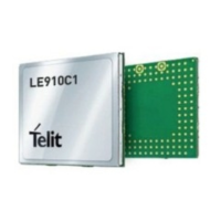
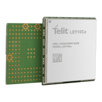
LE910Cx Hardware Design Guide
1VV0301298 Rev.40 Page 70 of 149 2023-03-16
Not Subject to NDA
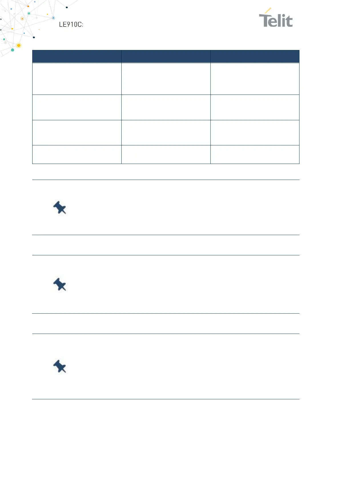
Table 26 lists the USB interface signals.
Signal Pad No. Usage
USB_VBUS A13 Power and cable detection for the
internal USB transceiver.
Acceptable input voltage range 2.5V
– 5.5V @ max 5 mA consumption
USB_D- C15 Minus (-) line of the differential, bi-
directional USB signal to/from the
peripheral device
USB_D+ B15 Plus (+) line of the differential, bi-
directional USB signal to/from the
peripheral device
USB_ID A14 Used for USB OTG to determine
host or client mode
Table 26: USB Interface Signals
Note: USB_VBUS input power is used internally to detect the USB
port and start the enumeration process.
It is a power supply pin with a maximum consumption of 5 mA.
Do not use pull up or a voltage divider for sourcing this supply
Note: Even if USB communication is not used, it is still highly
recommended to place an optional USB connector on the application
board.
At least USB signal test points are required as USB physical
communication is needed in the case of SW update.
Note: USB OTG feature is supported by default.
If the USB_ID pin asserted to ‘low’, USB OTG is enabled.
Please note that LE910Cx doesn’t supply 5V power to OTG devices
therefore an external 5V power is required on an application board to
provide 5V power to OTG devices.
 Loading...