LE910Cx Hardware User Guide
1VV0301298 Rev. 1.05 - 2017-06-18
Reproduction forbidden without written authorization by Telit Communications S.p.A. - All Rights Reserved
Telit Confidential Information, provided under NDA Page
98 of 117
10.4. Stencil
Stencil’s apertures layout can be the same as the recommended footprint (1:1). The suggested
thickness of stencil foil is greater than 120 µm.
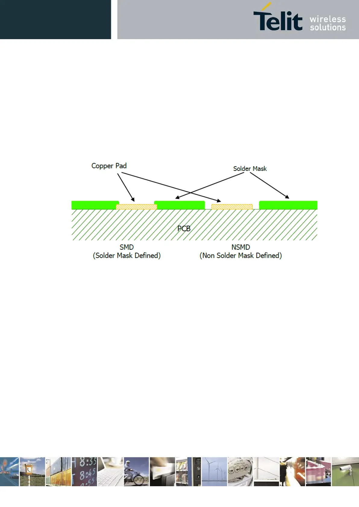
10.5. PCB Pad Design
The solder pads on the PCB are recommended to be of the Non Solder Mask Defined (NSMD) type.
Figure 25: PCB Pad Design