ME910C1 HW User Guide
1VV0301351 Rev.8 Page 13 of 99 2018-09-28
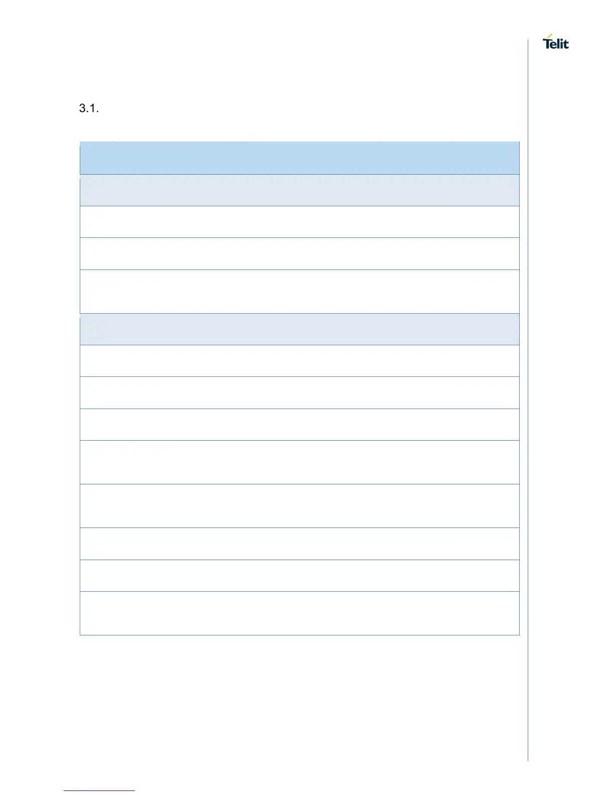
3. PINS ALLOCATION
Pin-out
Pin Signal I/O Function Type Comment
USB HS 2.0 COMMUNICATION PORT (FW upgrade and Data)
B15 USB_D+ I/O USB differential Data (+)
C15 USB_D- I/O USB differential Data (-)
A13 VUSB I Enable pin for the internal
USB transceiver.
5 / 3V Internal PD
(100K)
Asynchronous Serial Port (FW upgrade and Data with Flow Control)
N15 C103/TXD I Serial data input from DTE CMOS 1.8V
M15 C104/RXD O Serial data output to DTE CMOS 1.8V
M14 C108/DTR I Input for (DTR) from DTE CMOS 1.8V
L14 C105/RTS I Input for Request to send
signal (RTS) from DTE
CMOS 1.8V
P15 C106/CTS O Output for Clear to Send
signal (CTS) to DTE
CMOS 1.8V
N14 C109/DCD O Output for (DCD) to DTE CMOS 1.8V
P14 C107/DSR O Output for (DSR) to DTE CMOS 1.8V
R14 C125/RING O Output for Ring (RI) to
DTE
CMOS 1.8V
 Loading...