ME910C1 HW User Guide
1VV0301351 Rev.8 Page 81 of 99 2018-09-28
10. APPLICATION PCB DESIGN
The ME910C1 modules have been designed in order to be compliant with a standard lead-
free SMT process
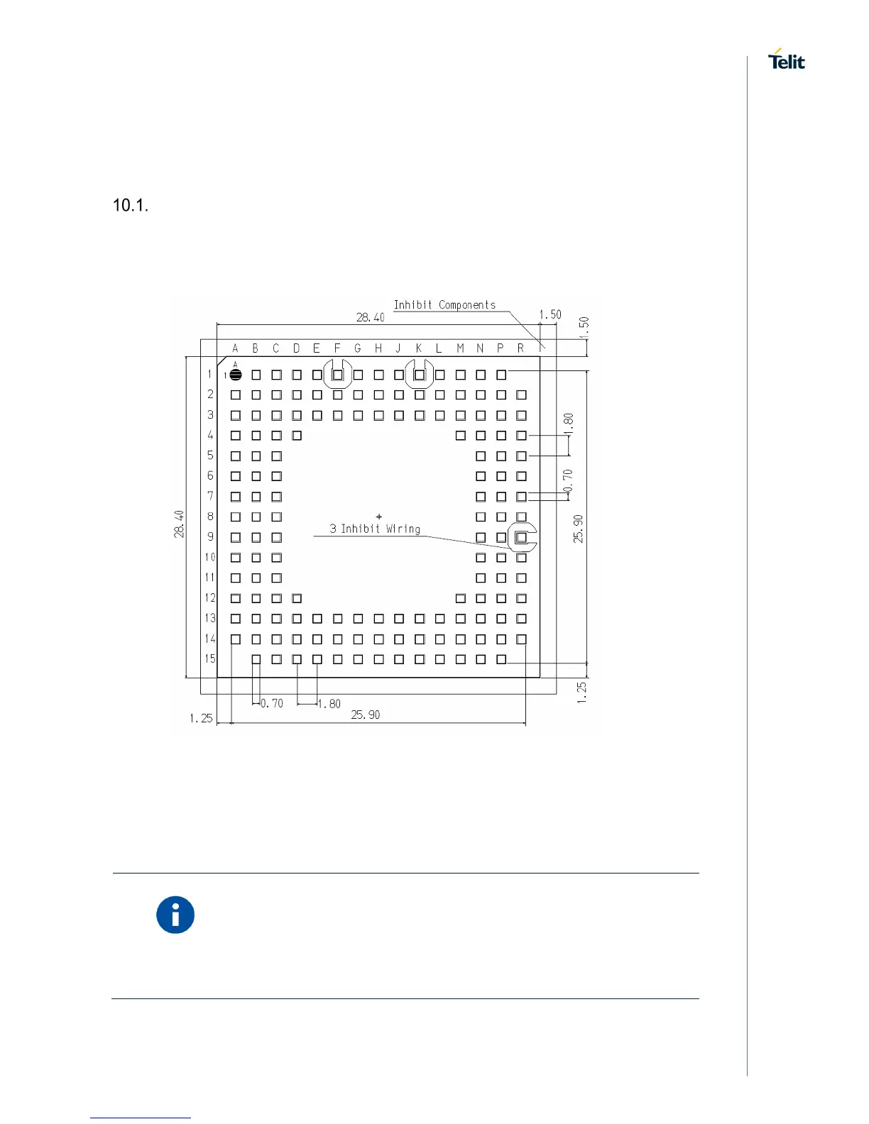
Footprint
TOP VIEW
In order to easily rework the ME910C1 is suggested to consider on the application a 1.5
mm placement inhibit area around the module.
It is also suggested, as common rule for an SMT component, to avoid having a
mechanical part of the application in direct contact with the module.
NOTE:
In the customer application, the region under WIRING INHIBIT (see
figure above) must be clear from signal or ground paths.
 Loading...