ME910C1 HW User Guide
1VV0301351 Rev.8 Page 71 of 99 2018-09-28
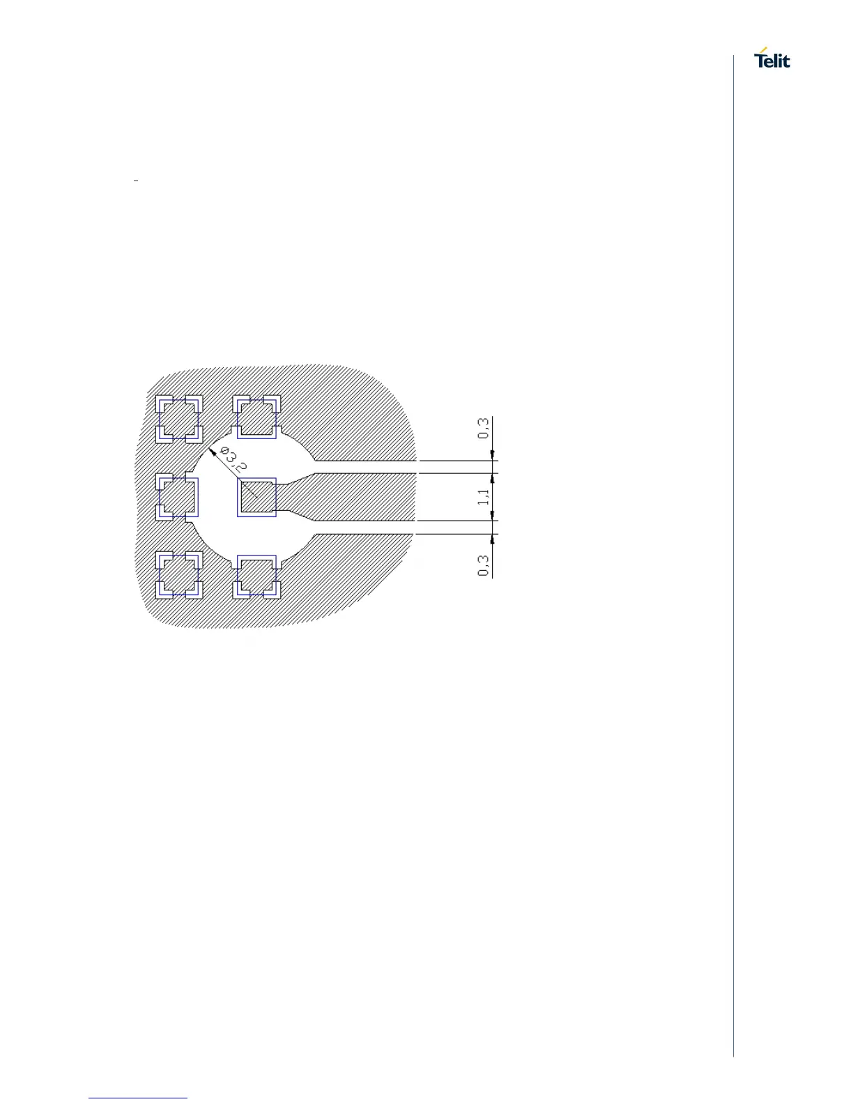
• If EM noisy devices (such as fast switching ICs, LCD and so on) are present on the PCB hosting the
ME910, take care of the shielding of the antenna line by burying it in an inner layer of PCB and surround
it with Ground planes, or shield it with a metal frame cover.
• If EM noisy devices are not present around the line, the use of geometries like Microstrip or Grounded
Coplanar Waveguide has to be preferred, since they typically ensure less attenuation if compared to a
Stripline having same length;
The following image is showing the suggested layout for the Antenna pad
connection:

 Loading...