22 Fm
To ADC Reference Inputs
VCAP1
10 Fm
VREFP
VREFN
Bandgap
2.4V or 4V
AVSS
R1
(1)
R3
(1)
R2
(1)
Using the ADS1298ECG-FE Software
www.ti.com
12
SBAU171D–May 2010–Revised January 2016
Submit Documentation Feedback
Copyright © 2010–2016, Texas Instruments Incorporated
ADS1298ECG-FE/ADS1198ECG-FE
3.4.2 Channel Registers Tab (ADC Register)
The Channel Register tab provides access to control registers that control different properties/settings for
the ADC channels. The control register are grouped into two groups: Global Channel Registers and
Channel Control Registers.
3.4.2.1 Global Channel Registers
The Global Channel Registers box includes Configuration Register 1 (CONFIG1), Configuration Register 2
(CONFIG2), Configuration Register 3 (CONFIG3), and Lead Off Control Register (LOFF). The upper half
of Figure 8 shows the section of the UI panel that allows manipulation and control of these registers.
Configuration Register 1 enables the user to control the resolution mode, enable the daisy-chain
configuration options, and program the data rate.
NOTE: Since the HR bit is not available in the ADS1198, the Configuration Register 1 control will not
show this control when testing the ADS1198.
Configuration Register 2 enables the user to select an internal square wave test source amplitude of
±1mV or ±2mV and a frequency of DC, 2Hz (f
CLK
/2
21
), or 4Hz (f
CLK
/2
20
).
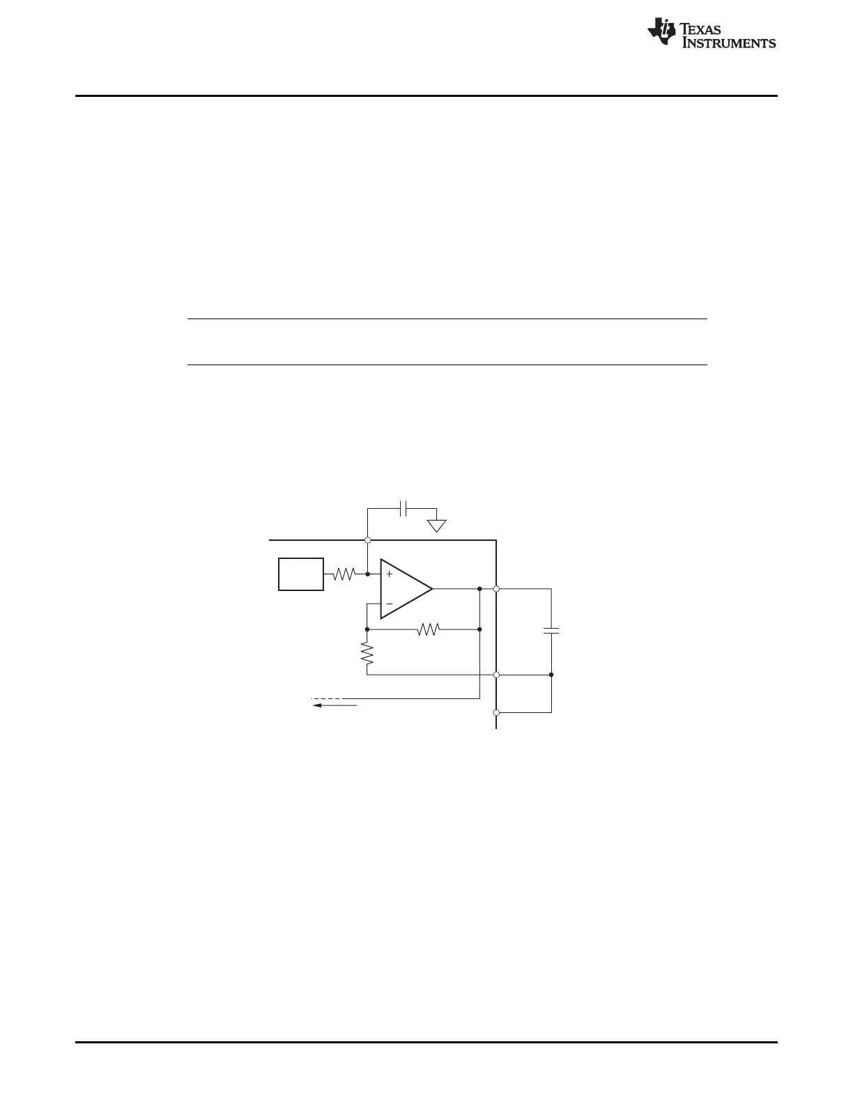
Configuration Register 3 controls the bandgap reference (illustrated in Figure 9) and right leg drive
(RLD) options. This register enables the user to select between an external or internal reference voltage,
enable/disable the internal reference buffer, toggle between a 2.4V or a 4.0V output voltage, and to
enable/disable the RLD as well as choose whether the RLD voltage is provided internally or externally.
Figure 9. Internal Reference and Buffer Connections
The Lead-Off Control Register allows the user to configure the threshold for the lead-off comparator,
resistive pull-up or current-source excitation, the lead-off current magnitude, and DC or AC detection.
Figure 10 illustrates a simplified diagram of the resistive pull-up and excitation options for the lead-off
detect feature.